> why does there seem to be a ground symbol on what I would think is the speaker output?
We normally run power output stages as emitter-followers, which is really Grounded Collector, ground at the battery CT. This is unity gain so it needs a hundred volts of drive signal.
We can also run Common Emitter. Ground at the emitters. The collectors fling the battery around and the battery CT is the "speaker hot". This only needs a few volts drive.
The difference is that in CE mode the driver is a 19 cent chip instead of some messy discrete collection.
The drawback is you can not run two channels from one battery.
Because this is wall-power, the conceptual "battery" is a PT winding, FWB, 2 Caps. All this must be duplicated for *every* channel.
At this insane power level, they would probably need many-multiple rectifiers and caps anyway, so the alternate topology does not add big-stuff cost and does reduce cost in the small stuff.
____________
I used to fix blown-up power amps for salary. _I_ would not begin to attempt this brute, especially with previous repair failures. Too much brain-work and smoked parts to suss-out what is *really* wrong. 3,500 Watt amps with warranty are not "that" expensive today (he says with a shudder).
Yet still another flying rail amplifier. In this case a big one. These amps weren't around very long - perhaps there is a reason. From what I've seen PV's flying rail amps go off like a brick of Black Cats when something goes wrong, many times taking out the whole thing. "Empty cans and charred remains" like Indianajo's PV 1.3k. You're lucky if just a couple of power transistors went out. The QSC (and clones) implementation is much simpler and less subject to catastrophic cascade fails.
QSC simpler? having been authorized service centyer for both brands, I feel exactly opposite. QSC circuits with commutating rails controlled by little surface mount housekeeping boards.
My experience is that when an output Xstr shorts C-E, one part blows, and maybe one on the other polarity. Might take out a driver. WHen one shorts B-C, then it takes out the entire row.
My experience is that when an output Xstr shorts C-E, one part blows, and maybe one on the other polarity. Might take out a driver. WHen one shorts B-C, then it takes out the entire row.
The circuit in question here is also commutating rail. Added onto a topology that some would question the wisdom of. IMO, there are only two reasons to do a flying rail - a) you really like lateral mosfets but you don't want to pay a voltage swing penalty, or b) you use CFP that you can directly ground the collectors of. This is neither, and only makes things more difficult than they need to be. Two power supplies, more crosstalk, and you don't even get to bolt the trannies to the heat sink without an insulator. And it's track record isn't as favorable as a standard Lin. Or the QSC flying rail.
The rail switches that I've seen the least amount of trouble with with is the 311 comparator on a bootstrap. When things do go wrong, there just seems to be less collateral damage. I've put those on 'standard ' amplifiers, and are almost fool proof. I've seen one and only one case where they just wouldn't work (and to this day never could figure out why not).
The rail switches that I've seen the least amount of trouble with with is the 311 comparator on a bootstrap. When things do go wrong, there just seems to be less collateral damage. I've put those on 'standard ' amplifiers, and are almost fool proof. I've seen one and only one case where they just wouldn't work (and to this day never could figure out why not).
Thanks All, for all the info!
I have only just grasped the Class H concept...and now 'Flying Rails'! I hate to reveal my ignorance (further) but I was actually thinking the ground symbol on the speaker output was just a link to some other connection point (or even a typo!).
I have a Crest CA-18 which has been tamed for home use (quieter fans installed and the noisy torroid dipped 20 times in electrical varnish)--I compared schematics and see that the Crest shares a common power supply for the low rails of channel A and B.
Indianajo;
Thanks for your info re 'flying rails'. It will take a few more coffees to absorb this, but at the very least, you have saved me tremendous confusion, right from the beginning. The next time I'm looking for victim, I will search for the schematic, not just the specs. If the primary advantage of this configuration is bridging, then I'm going to avoid it like the plague, if for no other reason than reduced damping factor.
PRR;
Thanks for your in-depth explanations also. I'm a little discouraged by your final remarks, but I bought this amp as a learning experience (and to be honest, I was hoping the repair might be something simple!) I've already learned a lot, and I'm not going to give up until it's an unidentifiable smoldering mass on the bench!
Enzo;
Thanks for your concise guidance on this project even before I have done the very basic 'legwork'. As soon as the boss's (wife's) head is turned, I will compare all devices, in circuit, comparing chan A to the functional chan B.
wg_ski;
Glad to have your input on this project, and thanks for your advice on my other projects. This amp has not appeared to have failed in a catastrophic manner---but I'm not done yet! BTW, with Class H amplifiers, is it not necessary to have devices insulated from the heat sinks anyway?, because of the multi-tiered rails, or am I 'out to lunch'.
BFN, Peter, in Hillsdale ON, Canada
Like any circuit, the insulation matters if the circuit demands it. QSC amps had their transistors "inside out", meaning the collectors were at the speaker common and emitters towards the powr rails. So with the "output" grounded for flying rails, we could ground the collectors, which is the part on the heat sink. But if the emitters are the common element, then the collectors still must be insulated.
Latest Update:
Tested in circuit it seems that Q 113, 115, 117, 119 and 121 are all dead shorted, Base to Emitter. This is the entire low rail PNP bank. Q 117 also appears to be shorted across all 3 pins. These five outputs where previously replaced.
I have read about "counterfeit" 2SA1302 transistors, but the bad outputs look identical, in every way to the remaining original transistors, except there is small arc bent into the leads, (I presume to allow for thermal expansion, avoiding stress on the PCB?).
OK: On removing 3 of the outputs (the other 2 to be removed anytime now) It seems that 2 of transistors are still good....I feel foolish for not realiziing that if one device shorts, they all appear shorted! (at least, Base to Emitter, I think).
I was about to smash open one of the defective trannies, and thought to do a quick, 'out of circuit test. It was still good! I will attempt to open the shorted device to compare it to an on-line video showing the so-called 'counterfeit' device's smaller chip size.
If the replacement devices where authentic Toshiba parts, then I am banking heavily on the problem being non-matching (un-balanced current sharing) in the second set failing.
I will draw indianjo's test rig, for selecting matched transistors and attach, asap....There is also some question as to the best substitute for these units, I read that they have been discontinued. Any input on the 2SA1302 debacle would be greatly appreciated!
Thanks again, Peter
Lacking input from Turk182 Enzo or other amp repair pros, I'd say attack the obsolete part problem by buying from Peavey parts dept. If they will sell you a few, then they think their matching program is good enough. If they insist on the whole set of channel outputs being replaced, then that proves they didn't solve the obsolescence problem either.
IMHO requires a phone call, I don't think they respond to internet orders.
I replaced all 20 outputs on my PV-1.3k with something cheaper than MJ15024/25, realizing that the bias spreader resistor value suggested by peavey might be wrong now. I used MJ21193/4 which is about $1 each cheaper with better SOA.
I have to say if you didn't do an Iceo test on each output to check if the junction is stessed, you don't know how many bad ones you really have. Just because they pass a double diode DVM test doesn't mean much. My stressed ones leaked too much current even at 12 v Vce.
Last edited:
Hi Indianajo and all;
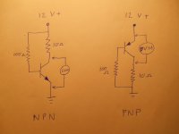
Before I even have all the PNP output trannies removed, I realize I will be in the transistor matching business! Attached is my interpretation of your test circuit. I have a lot of homework to do on the subject but I would like to use this thread as study in output matching, at the moment.
"The hfe is the ratio of the Ic/Ib. Its the current gain of the transistor"
I gather that we are comparing V ce, rather than the current gain?
Also, using the test rig below, how much Voltage variation would be allowed, to consider the transistors matched?
Attachments
Match output transistor by vbe. Diode connect it, run a constant current thru it, measure vbe. Hfe match is less critical. Parts from the same lot are usually close enough, but you can get them closer - like 3 mv or less. Buy at least a rail at a time, sort by vbe and use the oddballs for drivers.
Hi wg_ski;
I am prepared to buy a dozen outputs, is this a reasonable batch size to find a matched set of 5? Besides the electrical characteristics, there may be a package size issue. The 2SA1302's case (TO-247) specs a width of 16.2 mm max. One suggested substitute is NTE2329, but the case width (TO3BL) specs max width as 20.57 mm.
I have measured my 2SA1302 devices at approx. 19 mm and it appears that a 20 mm device width may fit, (class H really fills up the heat sinks!) Could you elaborate or your 'diode connect' method. I will sketch a schematic from your description, and post it, thanks, Peter.
Thanks again Indianajo;
Your test rig seems simple enough to construct. I suppose I will find out by trial and error, but, regarding the 5 second timing issue, with the 'DUT' on a heat sink, would the device reach an equilibrium temperature, that would reduce the need for timing?
Attachments
I had the transistors on a little heat sink when I tested Vce @ gain 10. I used clip leads & dangly resistors, though.Hi wg_ski;
Thanks again Indianajo;
Your test rig seems simple enough to construct. I suppose I will find out by trial and error, but, regarding the 5 second timing issue, with the 'DUT' on a heat sink, would the device reach an equilibrium temperature, that would reduce the need for timing?
I'm an experienced musician, so counting off 10 beats of 120 bpm is nothing to me. I marched a lot of football game halftime shows at 120 bpm in high school. 6 seconds or 4 seconds would be as valid, but it takes a few seconds to get your hands away from the clip leads and look at the meter. Just be consistent.
NTE meets the most basic of specs when matching transistors. If the original has Ft or Cbo or soa specs on their datasheet, look for those on NTE's. ? Central Semi is about as bad.
Read the sticky thread "my transistors real or fake" on parts forum before trying e-bay or ala-baba for obsolete parts. Rochester will sometimes sell you $100 of something recently obsolete, genuine close-out parts.
Hi wg_ski;
I am prepared to buy a dozen outputs, is this a reasonable batch size to find a matched set of 5?
I have measured my 2SA1302 devices at approx. 19 mm and it appears that a 20 mm device width may fit, (class H really fills up the heat sinks!) Could you elaborate or your 'diode connect' method.
A dozen may or may not be - if you order less than a full rail (25) you may get remnants from several batches. Which is what you don't want. May be matched may not - you roll the bones. When you order in batches of 25, you almost always get full rails/tubes because it's easy to pull them from stock that way.
"Diode connect" means short collector to base. When you match by vbe when diode connected, you also get a loose match on hfe. Gross hfe mismatch will affect base current, which affect vbe.
Hi Folks;
Thanks for your patience, not able to putter with the Peavey this weekend! I realize that output transistor matching is a topic covered in a number of threads, even here at diyaudio.
My goal is to find a simple but 'universally' accepted method of output matching. My sketch in entry #31 shows the volt meter connected Emitter to Collector. I will retract this, as wg_ski's 'diode connection' method has been reiterated in other forums.
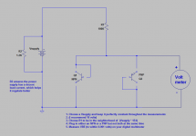
Here is a circuit which appeals to my simplistic nature. Not content to 'beat a dead horse', it must be completely 'fubar-ed'; R1 would allow a current of 0.1 mA, would it not be an idea to run the tests with this value, and again with an R1 that would allow a higher current ( 1 amp?)
Thanks for your patience, not able to putter with the Peavey this weekend! I realize that output transistor matching is a topic covered in a number of threads, even here at diyaudio.
My goal is to find a simple but 'universally' accepted method of output matching. My sketch in entry #31 shows the volt meter connected Emitter to Collector. I will retract this, as wg_ski's 'diode connection' method has been reiterated in other forums.
Here is a circuit which appeals to my simplistic nature. Not content to 'beat a dead horse', it must be completely 'fubar-ed'; R1 would allow a current of 0.1 mA, would it not be an idea to run the tests with this value, and again with an R1 that would allow a higher current ( 1 amp?)
Attachments
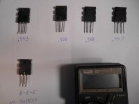
All five outputs of the PNP 'low rail' have been removed. I found only one device dead shorted E-B-C....Is this attributed to all the protection circuitry? When my Phase Linear 700's go 'fins up in the tank', there's usually 3 or 4 outputs shorted, and a smoking voice coil!
Agdr commented on my soon-to-be-vintage Fluke meter. It was just explained to me that the display reading in the diode-test mode may give some indication of matching. I suspect that this is far from sufficient and definitely not operating range current conditions, but what does it mean?
Here are my measurements with the fluke. I would appreciate all suggestions regarding the test set-up in the above entry (#39).
PS; I have readily available; a 12 V battery charger with large filter cap installed, a 13 V and 24 V regulated power supply, wondering if any of these are suitable. Timing regarding device heating is a major concern, as explained. I propose mounting all 'DUTs' on a large 1\2 " thick aluminum plate (with heat sink compound) if this is worthwhile.
Thanks again, Peter
Attachments
- Status
- This old topic is closed. If you want to reopen this topic, contact a moderator using the "Report Post" button.
- Home
- Live Sound
- Instruments and Amps
- Pet Peeve Peavey (GPS 3500)