I'm trying to convert this TS-5 to true bypass. I'm putting it in a new enclosure with a 3pdt switch, and I need to jumper the FET switching to always on.
Can any of you tell what points to jumper/what parts to remove on the following schematic?
http://www.freeinfosociety.com/electronics/schemview.php?id=1087
I appreciate any input.
Thanks,
Nathan
Can any of you tell what points to jumper/what parts to remove on the following schematic?
http://www.freeinfosociety.com/electronics/schemview.php?id=1087
I appreciate any input.
Thanks,
Nathan
Hey,
sorry for not replying, I got sick, and have been trying to keep up with school and work. Yeah, I suppose there is quite possibly a problem with the schematic. I was having some trouble following the circuit design based on this schematic, and I figured it was because I was a fool.
I don't know. I'm going to have to figure this out somehow. I did some research, and I know how a basic flip-flop circuit works (I know when Q=1 and Q'=0 is on, and the inverse is off), but I still don't know how you would wire it up to be always on.
What I think (which is admittedly, not worth much) is that in this schematic, Q1 is passing the signal for bypass, and Q2 passes the effected signal. Is that correct? If I want to wire a 3pdt switch, I would just remove Q1 and pass the bypass signal using the switch. Then, jumper Q2, and connect that 9v connector through the switch so the power connects with the switch, right?
Or am I completely misguided?
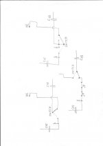
i don't see how to to edit my post. Anyway, this is what I mean. On all those arrows labeled "to switch" I would obviously have a wire coming back from the switch so that the switch would break lead when I switched it, I just didn't want to draw twice as many arrows. ")
An externally hosted image should be here but it was not working when we last tested it.
hello.
there are many possibilities,three are shown in the schematic.
be carefully,there can be errors in your orig. drawings.
i would measure up all points with a digitalmm and after that begin to build in or out something.
perhaps it helps...........
greetings.........
there are many possibilities,three are shown in the schematic.
be carefully,there can be errors in your orig. drawings.
i would measure up all points with a digitalmm and after that begin to build in or out something.
perhaps it helps...........
greetings.........
Attachments
- Status
- This old topic is closed. If you want to reopen this topic, contact a moderator using the "Report Post" button.