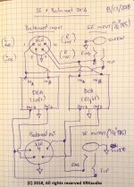
I've sketched a block diagram of what needs to be in the Balanced & Un-Balanced Amp / Headphone Switch chassis, that I've got in mind to assemble -
.

.
I know I can order the boards & parts to assemble the DCA Amps fairly easily, but the Balanced->Un-Balanced & Un-Balanced->Balanced, and Input & Output relay assemblies will need to be designed and built. I've begun drawing the schematics for the relay assemblies (on paper), but I guess I need to learn how to do the schematic capture in KiCAD, to generate a double-sided circuit board layout, with the correct footprints for all the parts (connectors, relays, diodes).
.
Which small production run board shops, in the USA, have you found to have the best quality & price for audio circuit boards? Thanks!
.
.
I know I can order the boards & parts to assemble the DCA Amps fairly easily, but the Balanced->Un-Balanced & Un-Balanced->Balanced, and Input & Output relay assemblies will need to be designed and built. I've begun drawing the schematics for the relay assemblies (on paper), but I guess I need to learn how to do the schematic capture in KiCAD, to generate a double-sided circuit board layout, with the correct footprints for all the parts (connectors, relays, diodes).
.
Which small production run board shops, in the USA, have you found to have the best quality & price for audio circuit boards? Thanks!
I've sketched a block diagram of what needs to be in the Balanced & Un-Balanced Amp / Headphone Switch chassis, that I've got in mind to assemble -
.
View attachment 696866
.
I know I can order the boards & parts to assemble the DCA Amps fairly easily, but the Balanced->Un-Balanced & Un-Balanced->Balanced, and Input & Output relay assemblies will need to be designed and built. I've begun drawing the schematics for the relay assemblies (on paper), but I guess I need to learn how to do the schematic capture in KiCAD, to generate a double-sided circuit board layout, with the correct footprints for all the parts (connectors, relays, diodes).
.
Which small production run board shops, in the USA, have you found to have the best quality & price for audio circuit boards? Thanks!
You might be able to do this via passive "switching" on the input/output TRS or XLR jacks.
Here is one approach to try... when using balanced, require a 4 pin XLR input jack to be used and 4 pin XLR output (to phones to be used) and wire accordingly.
When desiring to use unbalanced input and unbalanced output, use 3.5mm or 1/4in TRS input jack with right and left connected to only the +ve side of respective left DCA, and right DCA board. Correspondingly, the DCA board output on +ve side goes to right/left of TRS output jack. So basically, the negative (-ve) side of each DCA board is left unused when in unbalanced mode.
See attached schematic. Easy peasy... You could in fact power both balanced and unbalanced headphones simultaneously as amp has plenty of power to spare assuming impedance is not too low on either can. Since everything is cap-coupled, there is no fear of DC imbalance blowing something out.
Cheers,
X
Attachments
Last edited:
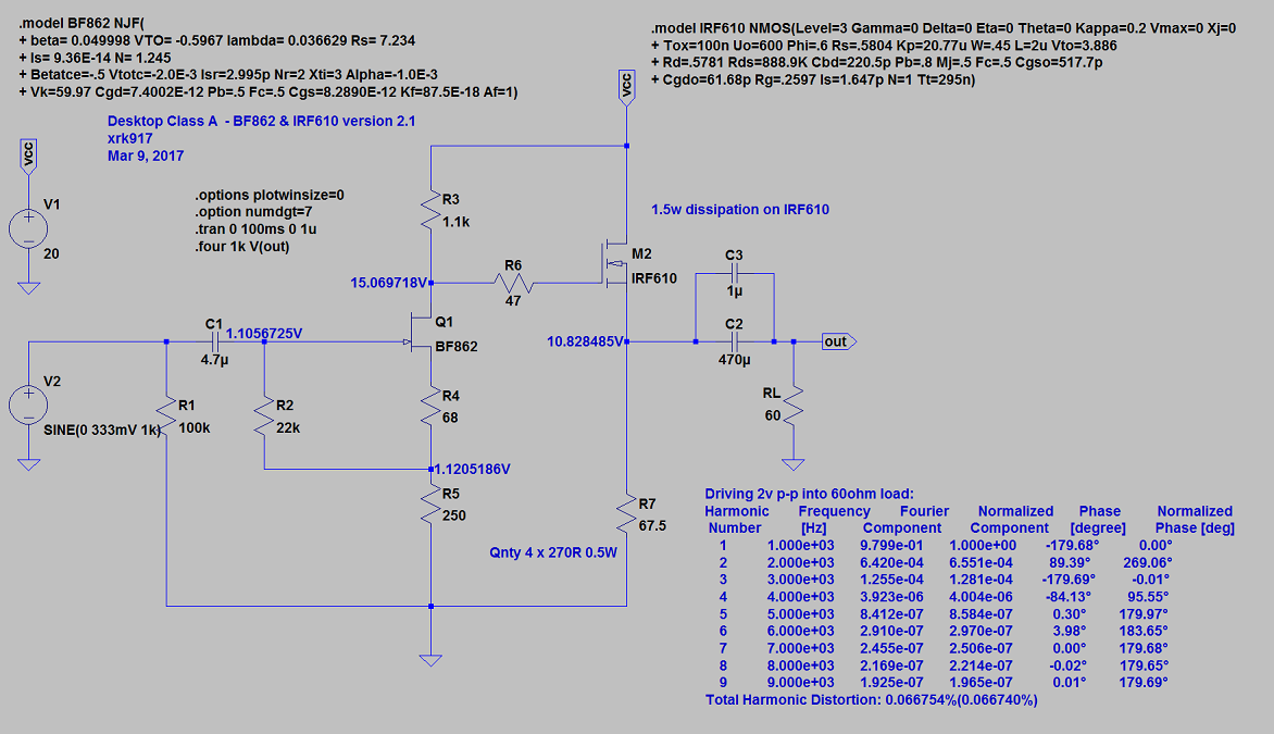
since my DAC has zero DC offset I tried bypassing input coupling caps and it is definitely better without the caps. they were 4.7uf jantzen standard caps... pretty expensive, so to put them to some use they replaced the 1uf Kemet bypass caps being used on the output. You would think the distortion of the electrolytic would swamp any improvement the higher quality cap could have here but there was a clear improvement over the Kemet (which was not a bad sounding cap to begin with).
maybe this is expected? they are in parallel so the signal has pathways through both caps, the parts of the signal lost through the electrolytic can pass through the PP bypass caps intact, if that makes any sense.
maybe this is expected? they are in parallel so the signal has pathways through both caps, the parts of the signal lost through the electrolytic can pass through the PP bypass caps intact, if that makes any sense.
The input coupling cap is not optional on this design as it allows the JFET to be properly biased by R4 and R5 divider - so the whole system DC setpoints are stable. What is your bias current through the 1k1 resistor with the input coupling cap removed? Also, what is the bias current through the main MOSFET through the resistor array with the input cap removed? If you change your volume pot without a coupling cap, that changes the DC setpoints. It’s interesting that you say it sounds better. Perhaps the bias setpoint increased?
The input coupling cap is not optional on this design as it allows the JFET to be properly biased by R4 and R5 divider - so the whole system DC setpoints are stable. What is your bias current through the 1k1 resistor with the input coupling cap removed? Also, what is the bias current through the main MOSFET through the resistor array with the input cap removed? If you change your volume pot without a coupling cap, that changes the DC setpoints. It’s interesting that you say it sounds better. Perhaps the bias setpoint increased?
I can check this tomorrow but there is no volume pot , volume is controlled digitally by the DAC.
dbaldock9 - you can draw the schematic in easyeda (online) and it can auto route the pcb for you. They are affiliated with jlcpcb and some parts site - so you can export for production straight to jlc and nab the boards for $2 + postage
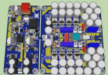
You mean combine both DCA’s onto a single board? You will have a hard time fitting that on 100mm x 100mm and it won’t be 2mm double thick copper with ENIG finish in order to get it for $2. But if you are ok with lower bias current one can basically make two Pocket Class A amps on a single 100mm square board. The DCA has a massive 150mA bias current that is capable of driving basically 99.9% of headphones out there. Only the HE6 might be an issue as it needs 2-3w power to realize its true potential. Really a full-size Class AB or Class A amp at 10w or more is the way to go in that case. Or go with my 8x parallel OPA1622 “Muscle Amp”. Still under development - Class AB using TI’s superb OPA1622 chipamp (WSON10 package). It’s capable of about 18wrms and is about 90mm x 100mm (not including PSU) but has double thick traces and ENIG. I have the boards just need to build it now.
Octal OPA1622 Muscle Amp:
Attachments
Last edited:
I thought dbaldock just wanted some boards for some relays..that was more what my suggestion related to
"Input & Output relay assemblies will need to be designed and built. I've begun drawing the schematics for the relay assemblies"
Is there a thread for your OPA1622 amp?
"Input & Output relay assemblies will need to be designed and built. I've begun drawing the schematics for the relay assemblies"
Is there a thread for your OPA1622 amp?
I thought dbaldock just wanted some boards for some relays..that was more what my suggestion related to
"Input & Output relay assemblies will need to be designed and built. I've begun drawing the schematics for the relay assemblies"
Is there a thread for your OPA1622 amp?
You are right, but I guess my reasoning was that all those relays were not necessary if you connect the input and output jacks like I showed above.
Here is the thread, it started as OPA1688 but I found 1622 later with double the current. Each one is capable of 140mA.
The thread got derailed with a bunch of of talk about bootstrapping the supplies but no one would give a schematic.
Cheap as Chips OPA1688 Low-THD Muscle Amp
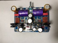
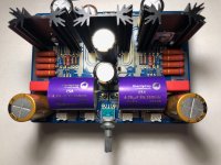
I've recently completed the DCA build but I'm having an issue I was hoping someone could help me "debug". I've already sent a message to XRK via Etsy about this but figured this may be of help to someone someday?
Decided to power the board using the DC-DC route connected to a 12V/1500mA Class 2 power supply. I've set the DC-DC to 20V for initial testing which when powered, the DC-DC has an illuminated LED. Connecting the DC-DC to the DCA causes the LED to extinguish and the voltage at the DC-DC output to drop to 0V. Removing the JST connector for the switch on the DCA causes the DC-DC's LED to illuminate once again and return to 20V. Shorting the switch causes a large spark (won't be doing that again!)
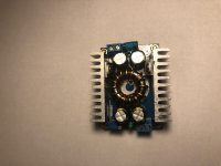
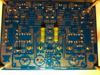
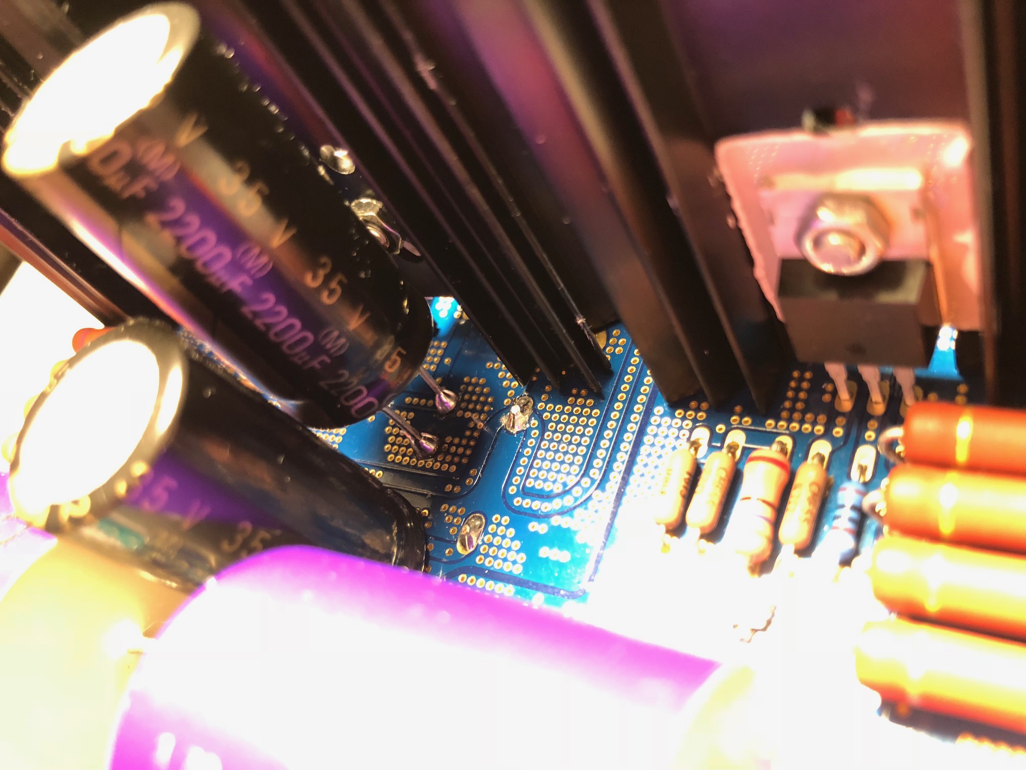
C134 stands slightly proud compared to the other caps as I had to remove the original cap in order to properly fit V132 to the heatsink, unfortunately I was unable to successfully remove the original pin stubs so I have soldered directly to the pads.
Please excuse the large underhanging resistors, I happened to have that value already and decided not to waste them!
I've included some photos in case I've missed anything obvious. Any help would be gratefully received.
Decided to power the board using the DC-DC route connected to a 12V/1500mA Class 2 power supply. I've set the DC-DC to 20V for initial testing which when powered, the DC-DC has an illuminated LED. Connecting the DC-DC to the DCA causes the LED to extinguish and the voltage at the DC-DC output to drop to 0V. Removing the JST connector for the switch on the DCA causes the DC-DC's LED to illuminate once again and return to 20V. Shorting the switch causes a large spark (won't be doing that again!)
C134 stands slightly proud compared to the other caps as I had to remove the original cap in order to properly fit V132 to the heatsink, unfortunately I was unable to successfully remove the original pin stubs so I have soldered directly to the pads.
Please excuse the large underhanging resistors, I happened to have that value already and decided not to waste them!
I've included some photos in case I've missed anything obvious. Any help would be gratefully received.
Attachments
-
 IMG_7455.jpg598.8 KB · Views: 118
 -
 IMG_7448.jpg420.5 KB · Views: 122
 -
 IMG_7452.jpg528.7 KB · Views: 489
 -
 IMG_7453.jpg567.6 KB · Views: 326
 -
 IMG_7458.jpg581.9 KB · Views: 314
 -
 IMG_7457.jpg594.3 KB · Views: 314
 -
 IMG_7456.jpg714.2 KB · Views: 326
 -
 IMG_7451.jpg657.4 KB · Views: 340
 -
 Shop.JPG155.5 KB · Views: 112
Last edited:
Hi RocketFox,
Sorry you are having trouble with this. I have had several people have this issue of sparks on startup. It must be that you have polarity reversed.
Here is the top view of the stuffing guide:
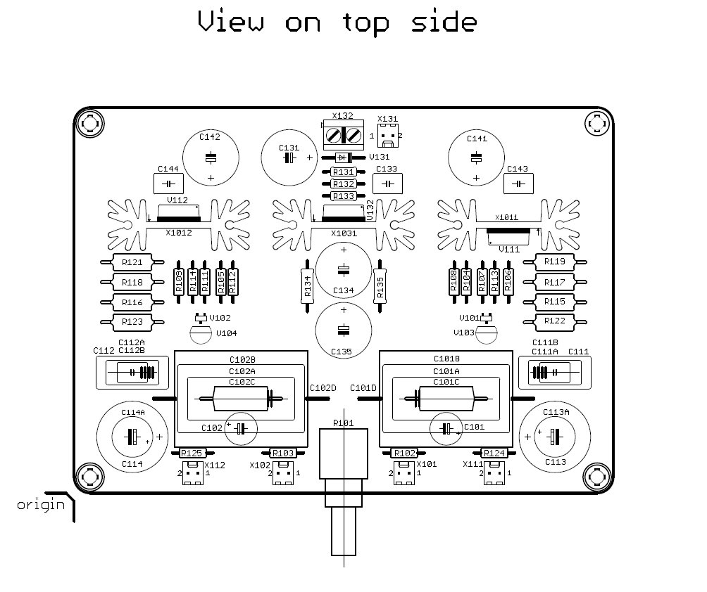
Note the '1' position of the power input terminal block (the one on the right, next to the JST jack). That's positive (+), and you can also verify as it is the pad that is not connected to the Swiss cheese ground plane. The JST jack is simply a switch and not connected to ground.
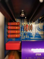
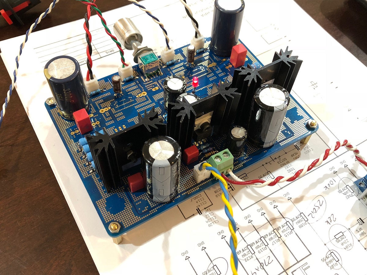
If you look at the photo of my build you can see where the red wire is, that's positive from the DC-DC step up. White is the GND from the DC-DC. Do you have yours connected in the same manner as this photo?
One other thing to check for is use a continuity checker to make sure your heatsinks are insulated from the mounting tabs on the MOSFETs. Else you get a short from +Vcc to GND - that will make a big spark too.
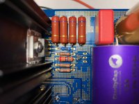
I do not see insulating shoulder washers on your MOSFETs - the bolt head should be on the MOSFET side and the nut on the other side. There needs to be a nylon insulating bushing/washer between the MOSFET tab and the screw head. The heatsink is grounded, and the tab is connected to Vcc via the cap Mx and CRC.
In photo of the cap Mx MOSFET, I see a short from Drain pin/tab to heatsink via the nut/bolt lacking an insulator. Take a DMM in continuity check mode and touch tab and GND plane - it will beep.
Luckily, no damage results as current simply flowed straight through the short and to GND. You need to remove the offending short and it will work.
Sorry you are having trouble with this. I have had several people have this issue of sparks on startup. It must be that you have polarity reversed.
Here is the top view of the stuffing guide:
Note the '1' position of the power input terminal block (the one on the right, next to the JST jack). That's positive (+), and you can also verify as it is the pad that is not connected to the Swiss cheese ground plane. The JST jack is simply a switch and not connected to ground.
If you look at the photo of my build you can see where the red wire is, that's positive from the DC-DC step up. White is the GND from the DC-DC. Do you have yours connected in the same manner as this photo?
One other thing to check for is use a continuity checker to make sure your heatsinks are insulated from the mounting tabs on the MOSFETs. Else you get a short from +Vcc to GND - that will make a big spark too.
I do not see insulating shoulder washers on your MOSFETs - the bolt head should be on the MOSFET side and the nut on the other side. There needs to be a nylon insulating bushing/washer between the MOSFET tab and the screw head. The heatsink is grounded, and the tab is connected to Vcc via the cap Mx and CRC.
In photo of the cap Mx MOSFET, I see a short from Drain pin/tab to heatsink via the nut/bolt lacking an insulator. Take a DMM in continuity check mode and touch tab and GND plane - it will beep.
Luckily, no damage results as current simply flowed straight through the short and to GND. You need to remove the offending short and it will work.
Last edited:
dbaldock9 - you can draw the schematic in easyeda (online) and it can auto route the pcb for you. They are affiliated with jlcpcb and some parts site - so you can export for production straight to jlc and nab the boards for $2 + postage
Thanks for the recommendation.
Once I've figured out the details I need for the different circuits, I'll begin the electronic schematic captures.
Hi RocketFox,
Sorry you are having trouble with this. I have had several people have this issue of sparks on startup. It must be that you have polarity reversed.
Here is the top view of the stuffing guide:
Note the '1' position of the power input terminal block (the one on the right, next to the JST jack). That's positive (+), and you can also verify as it is the pad that is not connected to the Swiss cheese ground plane. The JST jack is simply a switch and not connected to ground.
If you look at the photo of my build you can see where the red wire is, that's positive from the DC-DC step up. White is the GND from the DC-DC. Do you have yours connected in the same manner as this photo?
One other thing to check for is use a continuity checker to make sure your heatsinks are insulated from the mounting tabs on the MOSFETs. Else you get a short from +Vcc to GND - that will make a big spark too.
I do not see insulating shoulder washers on your MOSFETs - the bolt head should be on the MOSFET side and the nut on the other side. There needs to be a nylon insulating bushing/washer between the MOSFET tab and the screw head. The heatsink is grounded, and the tab is connected to Vcc via the cap Mx and CRC.
In photo of the cap Mx MOSFET, I see a short from Drain pin/tab to heatsink via the nut/bolt lacking an insulator. Take a DMM in continuity check mode and touch tab and GND plane - it will beep.
Luckily, no damage results as current simply flowed straight through the short and to GND. You need to remove the offending short and it will work.
Hi X,
Adding the insulating washers certainly stopped the sparks, thanks!
Finished the build again however I'm now noticing a few strange things:
1) With a source playing I can hear output even with the DC-DC disconnected, very faintly, this continues with the DC-DC connected and powered and only increases in volume near the end range of the volume pot but only slightly.
2) Every 4 seconds the volume suddenly decreases -the voltage output at the DC-DC drops in tandem with this decrease from 20.2V to around 11V for a second then begins to rise back to 20.2V before repeating the cycle again.
3) The switch has no effect.
Hopefully I haven't killed it! Any input gratefully received!
Last edited:
Sounds like your cap multiplier mosfet is dead. You can tell if it’s working if the voltage after it at the CRC rises slowly over 10 seconds. If it’s not working and always on - shorted, it doesn’t ramp up and the DC-DC supply shuts off cyclically due to inrush current to those caps. If you can hear music faintly it probably means your main MOSFETs are bad as well as the sound you hear is simply JFETs playing straight to the output with no amplification. Check for bad mosfet by measuring resistance between D&S should be in 10kohms not single digit ohms.
Replaced all three MOFSETs but unfortunately I'm still getting the same issue. Think I'm going to need to start again with a fresh board as had issues clearing the solder from the MOFSET holes and ended up being forced to surface mount.
Hi X,
None of the voltages rise slowly, all fluctuate at about the same interval. I've measured the voltages across the resistors and caps, hopefully this might shed some light.
Noticed V132 and V111 get warm quickly but V112 stays cold, this has been the case with both of the MOSFETs used.
None of the voltages rise slowly, all fluctuate at about the same interval. I've measured the voltages across the resistors and caps, hopefully this might shed some light.
Noticed V132 and V111 get warm quickly but V112 stays cold, this has been the case with both of the MOSFETs used.
Attachments
Last edited:
Rocketfox,
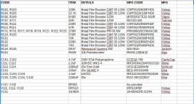
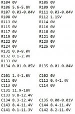
It would be helpful if you took the schematic and labeled the voltages you measure on the schematic. It's too time consuming and prone to errors on my part to transcribe your typed out values. Best would be to show voltage at each node relative to GND, not difference across them unless specifically for resistor arrays (R116/118/121/123 or R104/106/107/113, or for R106/109 so that we can see what the bias current across the MOSFETs and JFETs are, respectively. Most important is the voltage at the 3 pins to the two output MOSFETS V111/112 (Gate=1/Drain=2/Source=3). If the amp is working correctly, Drain should be same as voltage out of cap Mx R135 circa 20v, Pin 3 (Source) should be about 1/2 that voltage circa 9v to 10v, and pin 1, the gate should be about 14-15v. If these voltages are correct, the amp is biased in Class A and will make sound, almost guaranteed. If voltage of Gate is high and same as Drain but Source is close to 0v, then there is a problem on the JFETs biasing (probably incorrect resistor value (too big somewhere) or a cold solder joint and no current in JFET which should be around 7mA.
If working, all three MOSFETs get warm as V132 (middle one) is the cap multiplier and handles current for both channels (300mA) so 0.3Ax4v=1.2w (warm). V112 and V111 are the output MOSFETs and have a drop of 1/2Vcc or 10v x 0.15Amp=1.5w (a bit warmer than the middle one but close).
If the cap Mx works, then the voltages rise slowly and you can see this if an LED is connected to the output of the cap Mx at leg of R135.
Last edited:
- Home
- Group Buys
- xrk971 Desktop Class A (DCA) Headphone Amp