Hmm, controversial.
Check the data sheet curves.
It's a long data sheet. Which Fig # are you referring to?Check the data sheet curves.
Besides, you'll probably find the output Z is lowered by Cn at higher frequencies too.
It's a long data sheet. Which Fig # are you referring to?
Figure 46.
That explains it, thx. Die area = cost pressure from The Man?Die area, and (my secret) it brought out an internal node for playing. Why have 8-legs if you don't use them all?
")
I am predisposed to consider the nulling facility a bit of a red herring when compared to other NFB topologies. In HEC, for example, Cordell (probably unwittingly) essentially made a circuit that was already compensated such that the null just allowed adjustment around the compensated point; a bit of a gimmick. Your scheme is not the same so I'll think about it after I've taken the rubbish out. Life is one chore after another.
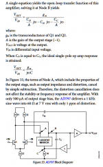
I think this refers to C1 on page 15 of the AD797 data sheet. I think this thread is talking about C2 (also Cn in fig 33), if so this paragraph applies:The distortion reduction capacitor is really only useful for high gains >100 times.
With your low gain circuit, the distortion will be well below the noise level,
and the capacitor will not be helpful.
The unique design of the
AD797 provides cancellation of the
output stage’s distortion. To achieve this, a capacitance equal to
the effective compensation capacitance, usually 50 pF, is connected
between Pin 8 and the output (see C2 in Figure 45). Use of this
feature improves distortion performance when the closed-loop
gain is more than 10 or when frequencies of interest are greater
than 30 kHz.
Edit: actually, I think we are both right. It isn't clear to me whether FritzS is asking about C1 or C2 or both. Probably both. So you are probably right that C1 is unecessary in his circuit.
Scott wrote the data sheet heck knows why I am trying to provide answers.
Last edited:
Edit: actually, I think we are both right. It isn't clear to me whether FritzS is asking about C1 or C2 or both. Probably both. So you are probably right that C1 is unecessary in his circuit.
Scott wrote the data sheet heck knows why I am trying to provide answers.
I think only about C1, the gain of the WNA is lower than 10 (fig. 46, page 15).
The schema of the WNA are a bit similar to the fig. 50 (page 16).
The NFB resistors of are 1kOhm (-in to ground) and 3.3kOhm (Vout to -in)
Between out (pin 6) and driver in are a J2 Murata Ferrite bead (initial designed for the 'diva' LM6171).
Fig. 50 (page 16) - Another open question, is the capacitor 22pF absolutely necessary in parallel to the resistor?
I haven't noticed any impairment of the sound, not even in comparison with the other OPAs already used in this amplifier.
My questions serve to sound out possible improvements.
I use the headphone amplifier mainly with the AKG K812, which in my experience reveals errors relentlessly.
The WNA is older now (own built 2005/2006), but I want to keep it for a while.
I don't know if I'm gonna build myself a new one or buy one. I don't want to do anything with SMD soldering anymore.
I recently borrowed Jan Meier's Corda Classic -ff, which is equipped with AD797 and on his published photos you can also see Styroflex capacitors.
This inspired the AD797 in the WNA. With this change (previously an OPA627 was inside), the WNA came quite close to the Corda. In the low frequency range the Corda -ff was in front. If you compare the power supplies of both it's not surprising.
Jan Meier knows my test report. Jan published DIY projects in no longer existing HeadWize Forum some time ago.
DIY Projects | HeadWize
PS: If my English is not perfect, my mother tongue is German.
Last edited:
Dennis Colin use in "LP 797 Ultra-Low Distortion Phono Preamp" (published in AudioExpress) a 47pF cap on each AD797 too.
Low Noise Design Schematics
HPS 1.0 Schematic
HPS 2.0 Schematic
Low Noise Design Schematics
HPS 1.0 Schematic
HPS 2.0 Schematic
@Scott
Dealing with garbage last night inspired me. I recommend it.
I find that a pernicious infinity has snuck invisibly in to your Fig 33 equation. No surprise. We knew the formula is not entirely realistic, after all it predicts an output in the absence of an output stage.
BTW, minor quibble, the Fig 33 formula may have a stray minus sign; when Cc=Cn the op-amp seems to be inverting?
Brian
BTW, minor quibble, the Fig 33 formula may have a stray minus sign; when Cc=Cn the op-amp seems to be inverting?
Brian
The original data sheet text (pre pdf days) was in something like Framemaker MIF or maybe an early Apple equation editor with extended ascii. Lots of errors crept in the most common one is lower case m instead of the MICRO SIGN.
@Scott: The AD797 is a clever design, of course. Not least the use of capacitors to provide output stage feedback, as opposed to resistors, making the system less voltage level dependent whilst facilitating bandwidth adjustment. Having user-adjustable internal stage feedback is unusual too, I believe (I rarely use opamps). The audible performance (not the primary target market) is capacitor dependent and arguably more problematic than using resistors.
FritzS’ question about the type of external C1 to use is interesting. It has me thinking about whether there are any subtle implications of paralleling caps via a current mirror.
FritzS’ question about the type of external C1 to use is interesting. It has me thinking about whether there are any subtle implications of paralleling caps via a current mirror.
Last edited:
I have a specific question.
In Fig 45, C1 is shown connected between pin 8 (node A in Fig 33) and ground. However, the dominant pole capacitor which C1 is "subtracting" from (Cc) is connected internally between node B and Vss (pin 4).
Why isn't C1 connected between node A and Vss (pins 8 and 4)?
In Fig 45, C1 is shown connected between pin 8 (node A in Fig 33) and ground. However, the dominant pole capacitor which C1 is "subtracting" from (Cc) is connected internally between node B and Vss (pin 4).
Why isn't C1 connected between node A and Vss (pins 8 and 4)?
Attachments
I have a specific question.
In Fig 45, C1 is shown connected between pin 8 (node A in Fig 33) and ground. However, the dominant pole capacitor which C1 is "subtracting" from (Cc) is connected internally between node B and Vss (pin 4).
Why isn't C1 connected between node A and Vss (pins 8 and 4)?
They're all AC ground, and any external cap has no extra parasitics. If your bypassing is poorly managed it "might" make a difference.
Famous last wordsThey're all AC ground,
Also, would connecting C1 to Vss provide some benefit to PSRR?
Are there any downsides to this?
This confused me earlier as these cap values are for C2, not C1. So I thought you were asking about capacitor types for C2.Now I will spend them the suggested 'Distortion Cancellation and Bandwidth Enhancement' caps, 47pF or 56pF (which are better?).
The data sheet examples use a max C1=33pF, presumably because higher values will cause increasing instability.
To optimize distortion you want C2 = 50pF - C1.
So C1 will not be the same value as C2 unless they are both 25pF and will probably need to stay below 33pF, unless Scott says otherwise.
Famous last words
Also, would connecting C1 to Vss provide some benefit to PSRR?
Are there any downsides to this?
With care in getting the bypass return current right it should not matter, easy to try. BTW if you look at the AD8010 data sheet the slightly unusual bypass arrangement was absolutely necessary to meet the video diff-phase spec. I spent a week building dead bug boards and cutting leads to a mm trying to get a normal arrangement to work.
On the bandwidth enhancement, yes you can make an oscillator at 50pf there is no net compensation. This part of the DS is a little esoteric and the values were empirical you'll have to experiment.
Last edited:
- Status
- This old topic is closed. If you want to reopen this topic, contact a moderator using the "Report Post" button.
- Home
- Amplifiers
- Headphone Systems
- Headphone Amp - AD797 compensation, distortion cancellation caps