Again - thanks everyone! I'm really enjoying the process of iterating this design, and am learning loads with each version. The feedback is hugely appreciated.
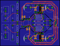
Here's the 4th draft:
Big capacitor problem
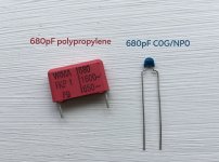
@OlegSh: The 680pF problem cap (a red WIMA polypropylene beauty) is of course pretty large. In my stash I also have some teeny tiny 680pF C0G/NP0 caps. In this case, would the smaller C0G/NP0 caps be a better choice, despite polypropylene ostensibly being cleaner in the signal path?
X7R 22uF caps
@00940: Thanks for the Murata reference! Checked out, and I see what you mean. I've also got some 10uF Samsung caps in the same package size. My idea then is to use a couple of these in parallel, and scrap the 22uF ones. Does this sound like a decent solution?
Thanks!
Here's the 4th draft:
- Schematic remains the same in this draft
- I finally moved the feedback resistors to the centre (between the ICs) as per @00940 and @OlegSh. As anticipated, this has shorted the feedback loops significantly (still learning how to visualise the loops, but getting there!) and shrunk the overall board size.
- Power traces slightly optimised again, with shorter runs and greater separation between rails
Big capacitor problem
@OlegSh: The 680pF problem cap (a red WIMA polypropylene beauty) is of course pretty large. In my stash I also have some teeny tiny 680pF C0G/NP0 caps. In this case, would the smaller C0G/NP0 caps be a better choice, despite polypropylene ostensibly being cleaner in the signal path?
X7R 22uF caps
@00940: Thanks for the Murata reference! Checked out, and I see what you mean. I've also got some 10uF Samsung caps in the same package size. My idea then is to use a couple of these in parallel, and scrap the 22uF ones. Does this sound like a decent solution?
Thanks!
Attachments
Last edited:
Do use any 680 pF caps.
Why not a discrete circuit?
Why the ground as a plane? Do define the "ground-paths". Plane the rest.
Just one input-ground.
To get a max. sound you have to listen and to tune ... a lot.
... for you: especially the psu;-)
- higher the capacity
- which capacitor
- bridge with little ones, or not?!
- where to set
- how to connect
...
- active or passive
- C-L-C or C-R-C...
...
LG
I am not with LG. PCB design does not involve guesswork and tuning by ear. I am pretty sure everything relevant for sound reproduction quality is measurable. If one needs an effect box they are readily available as separate devices. Designing equipment with built in "pleasing" distortion is not what I would call HQ audio. Also suggesting to manually laying out return paths is an old trend in audio design with star-ground and so on. The fact that many designers do not know how to use GND plane properly in their designs does not mean that it should be avoided in general. One still has to observe where return currents are going but it does not exclude using the solid GND plane for them. Also discrete vs integrated debate is not going to help OP with his current design. This is my opinion and everyone if free to disagree, I will not argue any further.
Now to the PCB layout in post #21. It is much better now but still can be made even better. Use a smaller NP0/G0G 680p capacitor. This cap has nothing to do with audio. The only concerns with it is that it should have low parasitic inductance and should not suffer from the microphonic effect, which is solved by using NP0/G0G dielectric.
Next, to be able to better explain you where to pay attention I would ask to put missing parts names on the PCB silkscreen (U1, U2, U3, R1, C1 etc). You can remove them later for production if you like it this way but it will help to refer to a specific part when discussing. When you upload updated PCB layout with parts numbers I'll write my further comments regarding the layout itself.
Regards,
Oleg
^ Completely agree!OlegSh: I am pretty sure everything relevant for sound reproduction quality is measurable.
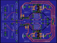
Thanks @OlegSh, attached is a version with (hastily) added silkscreen names, as well as a render that might be a little easier to read. Looking forward to your feedback as always!
Attachments
Last edited:
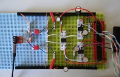
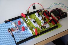
As an aside (and for those interested) I built a little breadboard prototype of the circuit. Here I used some electrolytics for the decoupling caps as my X7Rs haven't arrived from Mouser yet, and whatever approximate value resistors I could scrounge up. That gain resistor is 4.7kohm on each channel, making the gain around 5.7x in total.
Having spent the last hour or so listening to my usual test tracks with a decent set of cans, I'm extremely happy with the outcome. Crystal clear to my ears, no audible clipping when maxing out the volume, and a very subdued, soft power on/power off thump - far more tolerable than other breadboard amplifiers I've put together.
Considering a total lack of proper grounding, incorrect caps and shocking routing with needlessly long wires, it can only get better once the PCB gets a swing at it!
Attachments
Some comments to the layout in post #24.
If you turn U2 by 90 degrees clockwise and U3 counter clockwise you will solve some of the remaining issues with power supply routing. Note that when you turn U2 as I suggest you'll bring the CB2(L) closer to U1 negative supply pin which is good.
Do not route U1 supply traces all the way to the power entry connector since this increases power supply impedance for U1. Just connect all CA capacitors to their nearest CB capacitors on the same supply rail.
If you like you can make a provision for RC filter configuration by inserting a resistor in line with U1 supply pins (between CB and CA capacitors, CA caps should connect directly to the U1 supply pins).
You can rearrange input connectors such that they form a four way connector with two GND pins in the middle.
Rearrange RG0 and RG1 such that RG1 resistors are closer to the U2/U3 and RG0 are closer to the R3.
Once again, reduce the footprint of CIN2 capacitors.
After you’ve done all modification listed above, remove all GND plane cuts as they are no longer necessary since your power supply and signal paths do not cross. The supply return currents will follow the supply traces along the edges of the board. The signal return goes in the middle along the signal traces. Output can probably be improved by moving the R3s out of the middle to the left and turning them by 90 degrees. This bring one pin of R3 close to the corresponding buffer output. I think you can use smaller parts for R3 since power dissipation will most probably be negligible in normal headamp application if using low value resistors.
Regards,
Oleg
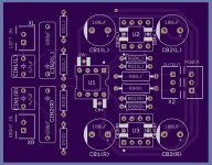
Thanks @OlegSh! As per your advice:
Apart from the fact that I still need to swap out CIN2 for smaller parts and get smaller R3 resistors, is this looking good from a ground/power supply perspective?
Thanks!
- U2 and U3 are rotated 90 deg. as suggested
- Power traces now run in only 2 separate rails each rather than 3
- Replaced input connectors with a single 4-way connector
- Swapped positions of RG0 and RG1
- Using a single, unbroken ground plane
Apart from the fact that I still need to swap out CIN2 for smaller parts and get smaller R3 resistors, is this looking good from a ground/power supply perspective?
Thanks!
Attachments
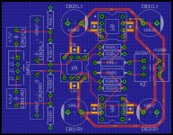
Looks much much better. Some more suggestions below.
1. Keep in mind that CIN2 and R1 ground pin should connect closer to the ground pins of the input connector. This is because signal return (R1) should go via shortest way to the source and RF interference should "leave" the board via shortest way (low impedance path) as possible.
2. If you have to cross the power traces do it near the power entry connector and not where U2 decoupling capacitor is connected.
3. If you have to use vias to the ground plane for decoupling capacitor you can swap the capacitor by a leaded version with 2.54mm pitch which will have similar impedance compared to the SMD part especially in combination with leaded IC and socket pins length. Also keep in mind that if you ever will need to remove/replace decoupling capacitors you will not be able to do it without damaging the IC sockets in your current layout due to zero clearance.
4. I overlooked the fact that the output pin of U3 is now at the left side, closer to the U1 which is not so good. Ideally you should turn U3 by 180 degrees to fix it but this will move the positive rail electrolytic capacitor away from U1 power pin which is not optimal but I guess should not be an issue considering overall short distances on the PCB.
5. Turn the R3's by 90 degrees such that they connect to the RG1's pins with a short trace.
6. Add four 3.5mm diameter mount holes at the corners of the PCB.
Regards,
Oleg
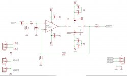
Quick question regarding the decoupling capacitors: Are the values I've got ideal?
I know @00940 mentioned that the 22uF X7Rs, given capacitance fluctuation due to voltage changes, would be less than ideal... and even 10uF caps would be better there.
I also read in this Analog Devices article that they recommend a very small (0.01uF - 0.1uF) close to the device and a larger (10uF - 100uF) cap further away, per rail.
While @JPS64 uses 0.1uF, 2.2uF and 100uF for each rail in his schematic.
Which values and types should I be using, assuming my current selection is less than ideal?
- 100uF electrolytics & 22uF X7Rs for the buffers
- 22uF X7Rs for the opamp
I know @00940 mentioned that the 22uF X7Rs, given capacitance fluctuation due to voltage changes, would be less than ideal... and even 10uF caps would be better there.
I also read in this Analog Devices article that they recommend a very small (0.01uF - 0.1uF) close to the device and a larger (10uF - 100uF) cap further away, per rail.
While @JPS64 uses 0.1uF, 2.2uF and 100uF for each rail in his schematic.
Which values and types should I be using, assuming my current selection is less than ideal?
- Status
- This old topic is closed. If you want to reopen this topic, contact a moderator using the "Report Post" button.
- Home
- Amplifiers
- Headphone Systems
- Critique my PCB! Headphone amplifier