 very nice!
BOM for Simple Discrete Regulator
Hello Patrick,
I downloaded the documentation package late yesterday, and it is complete, but with exception of BOM for the regulator. The text has footnotes to similar circuits, so I would have looked there to see values used, but the footnotes are not present either. I searched the forum for "simple discrete regulator" and only came up with 2 hits, neither of which apply.
I would prefer to buy values known to give 15V. I have very little "stock" of SMD parts, very few choices. If the regulator is from a previous group buy, I can look there. Maybe it's in this thread, but I quickly scanned the pages and did not find it. I know I'm missing something, but what?
Best regards,
Mike
I have a question about matching the CCS board BJTs. I have the following pairs:
Left channel: Q41=611, Q42=612, Q43=610, Q44=610 (Hfe value after the ”=” sign)
And the problematic Right channel: Q41=612, Q42=624, Q43=611, Q44=624
The problem is obviously with the bolded values since I have no more matches. Is it ok to match pairs like I proposed or should it be done differently? Otherwise I found quite good matches, but I seem to have run out of luck with the CCS devices.
Ok, thanks for the info. Please see attached my matching results for the Toshiba BJTs. I hope the results are adequate. The absolute Hfe values may not be correct due to my cheap DMM measuring accuracy, but at least I was able to repeat the measurements and get same values time and time again.
Let's hope this helps other builders.
Let's hope this helps other builders.
Attachments
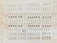
Actually excellent. Measured to 3 digits, matched to 0.16%.
What more can one want.
And no manufacturer would be able to afford this in a product.
Not even Nelson. Only DIY.
But if I were you, and you have 2 sets of boards, I would build a first set with less perfect devices.
Get them working as they should (first without servo and trim DC at CCS), do some listening.
Then rebuild the second set with your perfect devices.
You might well find that you do not need the servo anymore, which is all the better.
I did essentially the same, only first set with On Semi devices, then Toshiba / Sanken.
")
Patrick
What more can one want.
And no manufacturer would be able to afford this in a product.
Not even Nelson. Only DIY.
But if I were you, and you have 2 sets of boards, I would build a first set with less perfect devices.
Get them working as they should (first without servo and trim DC at CCS), do some listening.
Then rebuild the second set with your perfect devices.
You might well find that you do not need the servo anymore, which is all the better.
I did essentially the same, only first set with On Semi devices, then Toshiba / Sanken.
Patrick
I would build a first set with less perfect devices.
An excellent idea! I can't tell you how many times I've built the first with the best matched parts, only to find that my layout was wrong, or some design detail flawed, or power supply reversed and (lots of) magic smoke escaped. Followed by a second build with matches not as close. Doh!
I only have one set of boards, do you predict a second group buy in the near future?
The only PCB not tested was the CCS Bias daughter board.
But I have checked it 5 times to make sure no layout mistakes.
And You can actually test it separately first before soldering to the main amp board.
So little chance of a layout mistake.
I'll write a short procedure for the testing later.
If it happens to be not OK we shall replace them all at our cost including postage, as we always do.
I have limited boards (4) with me that have the silk layout "mistake" and only need a bit of resist scrapping.
Suggest you make and test one channel first with one of those if so wish.
You'll have to pay for postage.
Unfortunately I do not have enough to supply everyone.
So for those really unsure, perhaps wait for Morde's build.
He is usually real quick.
Patrick
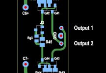
Test Procedure of the CCS Bias Daughter Board
To test the CCS Boas daughter board on its own :
1. Solder all components on board.
2. Connect a dummy resistor of 6.8k between output 2 (below Gnd pin, not labelled) and "C7-"
3. Repeat the same between output 1 (above Gnd pin, not labelled) amd "C6+"
4. Supply "C6+" with +15V, "Gnd" with 0V, and "C7-" with -15V.
5. Measure voltage drop across R45 to calculate JFET bias current. Should be 1.5mA +/-0.5mA.
6. Measure voltages across the two 6.8k resistors to calculate CCS bias. Should also be 1.5mA +/-0.5mA. And the two values should be identical to << 1%.
7. Remove the 6.8k resistors after test.
8. DC offset of the SL HPA can be trimmed later by adding a parallel resistor to either R42 or R44. Suitable pads already provided on the PCB.
Patrick
.
Attachments
Hello Patrick,
I have 100% confidence in your boards, it's my own boards I was referring to. I was just thinking "out loud" what a great idea to build a first set for testing/tweaking/tuning, and then a second set as final. Such a simple but practical approach. I don't know why but I've not considered that before. I will stay with Plan A and build the boards that I have, but in the future order 2 sets. Lesson learned.
Best regards,
Mike
Still wise to test CCS and main board separately.
The main boards can be tested with temporary resistors R9, 9a, 10, 10a as in the original schematics, before the marriage.
You of course need to remove them when replacing by the CCS board.
As long as you do not use a real headphone as load, and use a lab supply with current limit, nothing will happen.
See also post #138 of the GB thread.
Patrick
Last edited:
Thanks Patrick for providing guidelines to proceed with this build with less perfect parts first. It's just that the rest of the BJTs are quite far away from each other, but I guess it's better to make a practice build first and just have it producing sound.
By the way, what's a recommended power supply configuration for this build? I was thinking 2 x 20VA/2x17V toroid trafos (1 per channel), diode bridges, and CRCRC filter before the actual regulators. Could somebody hint me good diode models and values for the C/R? Something like C=10 000uF and R=0,47ohm perhaps.
By the way, what's a recommended power supply configuration for this build? I was thinking 2 x 20VA/2x17V toroid trafos (1 per channel), diode bridges, and CRCRC filter before the actual regulators. Could somebody hint me good diode models and values for the C/R? Something like C=10 000uF and R=0,47ohm perhaps.
- Home
- Amplifiers
- Headphone Systems
- The Pioneer Super Linear Circuit