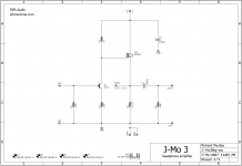
There are endless variations of this simple circuit changing the voltage, bias current, and JFET. I'm optimizing here for relatively low Z headphones and overall simplicity.
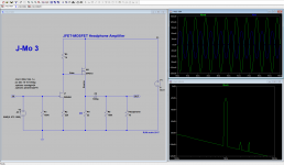
The gain is 6 dB. Output bias current is 100 mA.
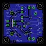
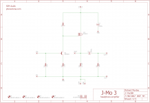
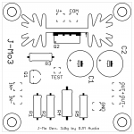
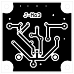
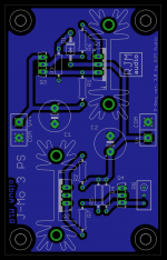
The circuit board is 50mm x 50mm.
Note: the LTSpice output distortion FFT is a little misleading as the JFET and MOSFET 2nd harmonic tend to cancel and how much cancellation depends on the headphone load and output signal. I just happened to hit a minimum at the simulation conditions shown. Typically it's about 0.2 % at -20 dB output.
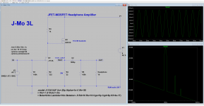
The gain is 6 dB. Output bias current is 100 mA.
The circuit board is 50mm x 50mm.
Note: the LTSpice output distortion FFT is a little misleading as the JFET and MOSFET 2nd harmonic tend to cancel and how much cancellation depends on the headphone load and output signal. I just happened to hit a minimum at the simulation conditions shown. Typically it's about 0.2 % at -20 dB output.
Attachments
Last edited:
")
Apparently the 2N5484 is obsolete and no longer stocked at Mouser, so I'm switching to the trusty J113.
It changes little. All we have to do is re-adjust R2.
The way this all works is as follows: The higher the supply voltage, the more gain you can squeeze out of the circuit. The lower the pinch off voltage (-V_gs0) of the JFET, the more gain you can squeeze out of the circuit.
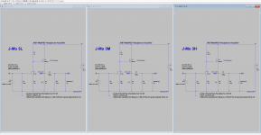
I'm working on parts lists for L,M, and H variants for low, medium, and high impedance headphones respectively.
The JFET you might use could have a slightly different operating point than the simulated result. That's where the TEST pad comes in. This measures the voltage on the MOSFET source, and if this is too low or too high then R2 can be raised or lowered respectively to bring the circuit back into balance. Most of the time the voltage will naturally be in the right range already, but it will catch any outliers.
Yes, you should roughly match the JFETs between channels. The tolerance does not have to be especially tight however.
Images attached for those who want to make a set of boards by transfer-printing method.
Gerber files attached if you prefer to let pcbway do the work for you. This is the single-sided version with no thermals.
It changes little. All we have to do is re-adjust R2.
The way this all works is as follows: The higher the supply voltage, the more gain you can squeeze out of the circuit. The lower the pinch off voltage (-V_gs0) of the JFET, the more gain you can squeeze out of the circuit.
I'm working on parts lists for L,M, and H variants for low, medium, and high impedance headphones respectively.
The JFET you might use could have a slightly different operating point than the simulated result. That's where the TEST pad comes in. This measures the voltage on the MOSFET source, and if this is too low or too high then R2 can be raised or lowered respectively to bring the circuit back into balance. Most of the time the voltage will naturally be in the right range already, but it will catch any outliers.
Yes, you should roughly match the JFETs between channels. The tolerance does not have to be especially tight however.
Images attached for those who want to make a set of boards by transfer-printing method.
Gerber files attached if you prefer to let pcbway do the work for you. This is the single-sided version with no thermals.
Attachments
Last edited:
BOM uploaded
fixed a few small errors, and revised the optional M and H configurations as shown below in the LTSpice sims.
"L" 5 dB gain, for 16-32 ohm headphones
"M" 12 dB gain, for 60-120 ohm headphones
"H" 18 dB gain, for 150-300 ohm headphones
Attachments
It is very nice to see the new design of j-mo. I am just wondering what is the difference between the j-mo 3 to its older brothers and sisters in terms of performance to >120 ohm headphone and will the power efficiency be a bit better? Would like to see one of the j mo sitting on my desk as the first attempt of a discrete headphone amp.
The original J-Mo was JFET buffer + MOSFET buffer, it had no voltage gain which was, well, less than ideal.
The J-Mo II added voltage gain using a compound JFET-bipolar input stage. It didn't work all that well at gains above 10 dB and because the circuit values were inter-dependent in a nonintuitive and complex way it was a pain to reconfigure.
The J-Mo 3 drops the compound transistor for a JFET voltage amplifier. The circuit loses some PSRR compared to the Mk. II, but it is much simpler both conceptually and operationally. It works fine with different headphones, but unlike more complex and full featured headphone amplifiers a single configuration won't be ideal with all headphones, it needs to be built in a configuration optimized for the range of headphone impedance its going to be used with. The upside is it is really tiny, dirt cheap, and as pretty near idiot proof as they come.
The output stage is unchanged since the beginning, but the power efficiency will vary on a case-by-case basis depending on the voltage, bias current, and load impedance. As a class-A output stage with resistive current source it is not going to win any contests on that front, no matter what, but the latest version does at least make an effort to optimize for different loading.
****
BOM 30g2 uploaded, tweaked "M" configuration values slightly.
Attachments
Last edited:
but certainly not the ultimate solution to whatever the problem is
Exactly this!
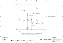
Regarding the power supply I have two suggestions, one easy, one less easy.
First the easy one: use a three-terminal fixed voltage regulator. It's enough to get the job done. (values in brackets refer to L/M/H versions of the J-Mo 3 respectively)
transformer with (9 / 12 or 2x6 / 18 or 2x9) VAC secondary winding, 25 VA or more
---> bridge rectifier
------>1000 uF
---------> 1-2 ohms
------------> 1000 uF
---------------> LM7809/7812/7818 with 10 W/C heatsink (will dissipate about 1 W)
------------------> 1000 uF
output is 9, 12 or 18 V DC.
maybe string an indicator LED off the output, use 1k~2k2 dropping resistor
if not an LED, 2k2 between output and COM as a bleeder resistor to drain off excess charge when the power is cut.
Yes, you can upgrade the LM780x ICs with LM317 or whatever you feel comfortable with.
The more complicated solution in next post.
The main boards already call for 1000 uF, so this cap just brings the total output capacitance for a stereo build up from 2000 uF to 3000 uF.
I remember there was some discussion of IC V-regs showing peaking when loaded with over 220 uF output capacitance.
While in general I agree with keeping capacitance on the light side, I'd recommend scaling that estimate according to the circuit current draw. If you would use 100 uF with an op amp at 5 mA for example, a circuit drawing 100 mA should see 2000 uF.
A MOSFET shunt-source voltage regulator, with better PSRR than your typical ICs. Under development.
Originally used configured as a phono stage power supply.
Originally used configured as a phono stage power supply.
Attachments
Yeah, I think a shunt regulator will be a better option than LM-series regulators with large output caps hung out on the end of them.
Having just built and tried the Jung/Didden super regulators with several circuits, the SQ is definitely improved over LM-series regulators at the expensive of added complexity.
Not sure how your MOSFET shunt-source regulator compares to the Jung regulator, though.
Press on Richard!
Having just built and tried the Jung/Didden super regulators with several circuits, the SQ is definitely improved over LM-series regulators at the expensive of added complexity.
Not sure how your MOSFET shunt-source regulator compares to the Jung regulator, though.
Press on Richard!
I have a question.
About the heatsinks - they have two retaining pins which in Eagle can be connected to circuit elements. Is it better to ground the heatsinks or leave them disconnected from the circuit? The former will require isolation from the MOSFETs, the latter allows the fet substrate to be in electrical contact with the heatsink...
About the heatsinks - they have two retaining pins which in Eagle can be connected to circuit elements. Is it better to ground the heatsinks or leave them disconnected from the circuit? The former will require isolation from the MOSFETs, the latter allows the fet substrate to be in electrical contact with the heatsink...
I have a question.
About the heatsinks - they have two retaining pins which in Eagle can be connected to circuit elements. Is it better to ground the heatsinks or leave them disconnected from the circuit? The former will require isolation from the MOSFETs, the latter allows the fet substrate to be in electrical contact with the heatsink...
I've always left the retaining pin pads disconnected from the circuit altogether.
Why would you want to ground them?
Why not to add a decoupling cap in series, at the signal input on board, for safety reasons?
Unless I'm misreading what you are suggesting, I don't see the need as the output of the circuit is not DC coupled. There is no way to damage the headphones leaving the input DC coupled, and the JFET has no gate current that needs to be isolated from the volume control.
re. the heatsink connection, I detect some difference in opinion in line with my own waffling ... I see the arguments for grounding it, but I also see its unlikely to offer much real world advantage. I suppose it comes down to whether anyone is likely to want to mount the FETs to the heatsink without electrical insulation.
- Home
- Amplifiers
- Headphone Systems
- JFET-MOSFET headphone amplifier J-Mo 3