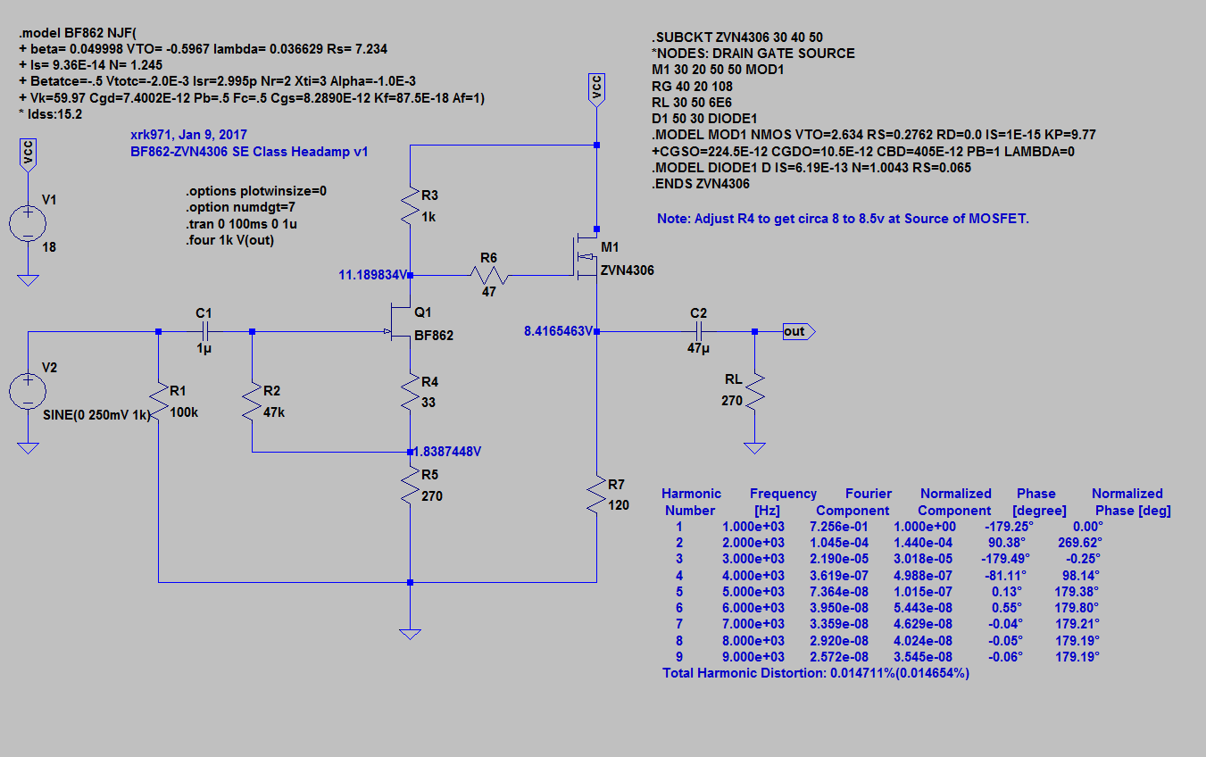
This should sound good. You might want to put 47R gate stopper on mosfet to prevent oscillations. Add some local feedback with a 47R to 33R between source and gare of JFET and you will get a harmonic distortion profile that is dominant H2 vs H3.
Then it looks a lot like this:
FFT is like this:
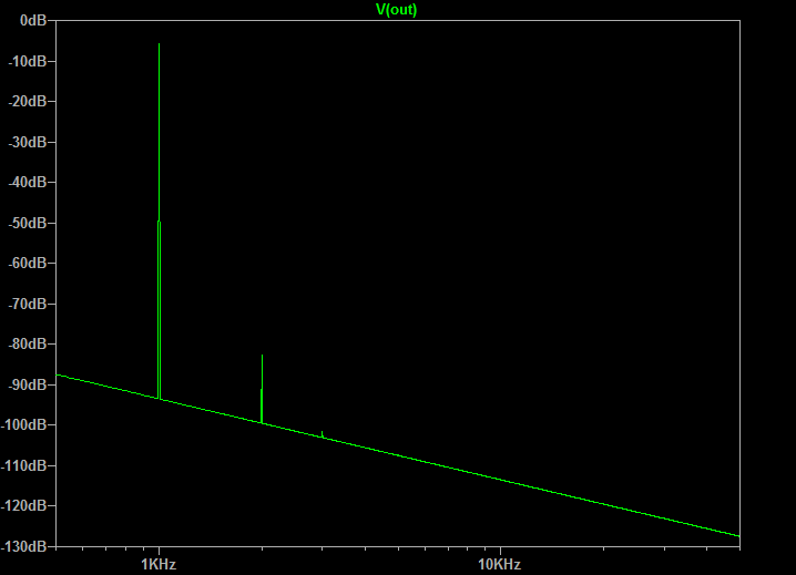
Then it looks a lot like this:
FFT is like this:
Hi XRK,
Before I posted this to diyaudio, I brought up your circuit on my G+ pages, here. Sorry, I should have repeated that shout out here too.
The J-Mo 3 is forking the J-Mo 2 with the JFET amplifier you used as the input, minus the "feedback" resistor ... which is not feedback by the way, it's just a way to bias the JFET and I figured I could get rid of both that and the input coupling cap if I could find a JFET and V+ combination that would give the right gain and bias without it.
About the MOSFET gate resistor, did you confirm your amp oscillated without it? Normally its only a problem with long leads and or negative feedback, neither of which apply here.
/R
Hi XRK,
Before I posted this to diyaudio, I brought up your circuit on my G+ pages, here. Sorry, I should have repeated that shout out here too.
The J-Mo 3 is forking the J-Mo 2 with the JFET amplifier you used as the input, minus the "feedback" resistor ... which is not feedback by the way, it's just a way to bias the JFET and I figured I could get rid of both that and the input coupling cap if I could find a JFET and V+ combination that would give the right gain and bias without it.
About the MOSFET gate resistor, did you confirm your amp oscillated without it? Normally its only a problem with long leads and or negative feedback, neither of which apply here.
/R
No, I never bothered to build it without the 47R gate stopper on the JFET. It seems to sound fine and measures very well so I see no need to change it. I am not fond of skipping bypass caps as you never know when your source may be loaded with DC. You can really get a nasty pop on the headphones when plugging in.
My circuit works very well with high impedance phones like 250ohms to 300ohms. Distortion is about 0.045% and mostly second harmonic with some 3rd and nothing else. With 2 9v batteries running about 55mA bias, the max power output into 250ohms is about 50mW (10v p-p) and still be under 0.5% THD. Many reports of high impedance phones like HD600, DT880, etc working very well.
I am not fond of skipping bypass caps as you never know when your source may be loaded with DC. You can really get a nasty pop on the headphones when plugging in.
You'll get a pop regardless of whether there's an input coupling capacitor there or not if you plug a source leaving the volume control turned up. (It's really not a good idea.) The output is AC coupled so there is no particular necessity** to have the input AC coupled as well provided the JFET gate is unbiased. In your version it is biased, and the input capacitor is needed for DC blocking.
** a large DC offset on the input will re-bias the MOSFET potentially causing it to overheat, so that's something that the input capacitor guards against. If that's a concern, it is best to add the input cap.
(A typical offset of 50 mV, through the volume control, 5 mV, amplified by the JFET, 50 mV, is not going to affect the circuit performance any, we are talking a failure case where 1 V or more is present on the input for some reason.)
Last edited:
Eagle files for the JMo3 and MReg2. You can make whatever changes you need and then run the CAM processor to make the Gerber files.
Attachments
Absolutely, yes. The configurations adjust the voltage gain, voltage headroom, and bias current to the optical value for the headphone impedance but everything will work with everything to all sensible volume levels. The main purpose of the three builds is to set up the ideal voltage gain for the headphones you most plan to use.
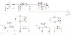
low cost desktop amp project based on JMO3
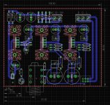
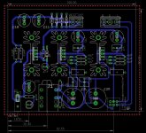
Have been thinking building a low cost desktop amp for working place. JMO3 was one of best candidate. I made first layout for 100mm*80mm PCB. Any recommendations or advices welcomed")
Have been thinking building a low cost desktop amp for working place. JMO3 was one of best candidate. I made first layout for 100mm*80mm PCB. Any recommendations or advices welcomed
Attachments
I like it.
1. It seems an odd place to put the power switch, after R10. I understand that it doesn't switch the AC, since the power brick is external, but is there any logic to having it after C10,11?
2. power terminal incorrectly labelled RGL.
3. C2R/L butt up right against the front panel.
4. is the volume control the correct outline? It doesn't show the mount or the shaft.
5. I would add a mm or so clearance between C14/C15 and similar.
6. is a Zener really better than a resistor for the adjustable voltage regulator?
Richard
Thank you, Richard!
Actually not.
I just wanted to keep power switch on front.
I will modify schematic and layout tonight.
Any other advice is welcomed
1. It seems an odd place to put the power switch, after R10. I understand that it doesn't switch the AC, since the power brick is external, but is there any logic to having it after C10,11?
Actually not.
I just wanted to keep power switch on front.
Do you have any reason with E-cap direction?3. C2R/L butt up right against the front panel.
I haven't measured it, but I read an article that using zener reduces output noise of LM317.. I don't know it is really better or not, but I decided to try since BZX55 is cheap.6. is a Zener really better than a resistor for the adjustable voltage regulator?
I will modify schematic and layout tonight.
Any other advice is welcomed
Last edited:
If you upload the eagle brd/sch files maybe I or someone else would volunteer to do some touch up.
I think it's basically fine though. Did you check it passes ERC/DRC?
Yes. I checked with Seeed studio DRU, no issue found.
I will upload eagle files tonight
- Home
- Amplifiers
- Headphone Systems
- JFET-MOSFET headphone amplifier J-Mo 3