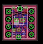
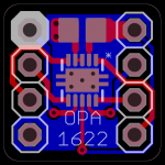
As written in my CMoy/Hello World thread I am interested in the OPA1622, which has one huge draw back for breadboard prototyping: VSON10 package with a 3x3mm (0.11"x0.11") footprint.
For the more common packages (e.g. SOIC8) adapter boards to DIP8 are available. But since there are only a few VSON10 chips available, there seems to be no commercial interest for these breakouts. To fix this, I started to design a breakout board of my own.
The VSON10 features two additional pins:
The first is a enable toggle. I routed it to an external connector, but also added a trace to V+ for "always on" (trace needs to be cut for external enable signal).
The other is a GND pin. The datasheet requests a clean, analog ground for best performance.
Having a GND connection on the board allowed me to do a ground fill (both top + bottom, but this required three vias for good results).
For best performance, the datasheet asks bypass caps to be as close to the IC as possible, thus I added spots for optional 0603 bypass caps to the board. Having spots for feedback resistors/caps on the board would also be nice (says the datasheet), but I don't think I could cramp them on there (and also, swapping 0603s for prototyping seems a tad bit too fiddly).
Also, the head dissipation plane (V-) on the back is already not that huge.
Before I build a 10x10cm grid (7x7 boards) I would like to ask opinions on the layout. This is the first time I did something like this ;-)
So do you think it's okay that way?
Or did I try too hard to prevent parallel lines?
Is the heat dissipation area big enough, or too little?
If I produce these I will probably set up a group buy. The 490 breakout boards would cost me 34US$ via dirtypcbs (or 60US$ with ENIG and quicker shipping to Europe). And I only need a few of these...
Question on producing: As I understand it, I need to put the 49 copies of my board onto a 10x10cm area and add lines for v-groove. Or is there are better/cheaper panelization option?
Some links:
OPA1622 thread on diyaudio: http://www.diyaudio.com/forums/vendors-bazaar/283672-new-audio-op-amp-opa1622.html
Datasheet: http://www.ti.com/lit/ds/symlink/opa1622.pdf
VSON10 package: http://www.ti.com/lit/ml/mpds117k/mpds117k.pdf
Attachments
Last edited:
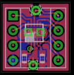
Interesting idea. A couple of suggestions if I may. I would rotate the OPA1622 by 180 degrees so that the V+ supply pin of the adapter board is closer to the corresponding OPA1622 pin. This way you can use the thermal pad to route the V- supply to the OPA1622 pin. As it is now the V+ trace is too long and this can be improved. I would also skip the enable pin connector and just add a resistor divider between V+ and GND to enable the IC once the power is ON.
Also if you make the entire bottom side a copper pour connected to the OPA1622 thermal pad you will greatly improve the cooling of the IC. GND connection is only needed next to the decoupling capacitors and thus you do not need it on the bottom layer since this will have little effect on the overall GND connection impedance, IMO.
I built some OPA1622-to-DIP10 adapters.
(PCB layout in post #76)
(test bench and testing results in posts #209, 210, 211)
(PCB layout in post #76)
(test bench and testing results in posts #209, 210, 211)
Oleg, of course you may ") I did a quick try at rotating the 1622 by 180 degrees, but wiring got really difficult. Sticking to the DIP8 op-amp pin out is really... not nice.
I did a quick try at rotating the 1622 by 180 degrees, but wiring got really difficult. Sticking to the DIP8 op-amp pin out is really... not nice.
But I did change the bottom plane to be V-, and could shorten V+ a bit.
See attached image.
Maybe I could put the OPA on the bottom. This would change the geometry and might enable a nicer solution (not sure if that's good for cooling, though).
Also, this could be a hassle in scenarios where height is an issue?
Will try that later, but neither today (was listening to music far too long and should get some sleep^^) nor tomorrow (gf anniversary).
Honestly, I don't know what benefit a resistor divider on the board would offer? If you could explain it, that would be nice
According to the datasheet, Enable can just be connected straight to V+ (what I did). So the IC is up if there's power, same as with divider. Additionally, if someone would like to use the enable feature [e.g. with resistor divider instead of direct connection], it's "exported" via the pin.
Mark, oh, yes, didn't see those. Also quite nice But I want to be able to use the OPA1622 in existing circuits with DIP8 sockets. I think plutonim did that, but his layout didn't seem to be easily available.
I did a quick try at rotating the 1622 by 180 degrees, but wiring got really difficult. Sticking to the DIP8 op-amp pin out is really... not nice.But I did change the bottom plane to be V-, and could shorten V+ a bit.
See attached image.
Maybe I could put the OPA on the bottom. This would change the geometry and might enable a nicer solution (not sure if that's good for cooling, though).
Also, this could be a hassle in scenarios where height is an issue?
Will try that later, but neither today (was listening to music far too long and should get some sleep^^) nor tomorrow (gf anniversary).
Honestly, I don't know what benefit a resistor divider on the board would offer? If you could explain it, that would be nice
According to the datasheet, Enable can just be connected straight to V+ (what I did). So the IC is up if there's power, same as with divider. Additionally, if someone would like to use the enable feature [e.g. with resistor divider instead of direct connection], it's "exported" via the pin.
Mark, oh, yes, didn't see those. Also quite nice
But I want to be able to use the OPA1622 in existing circuits with DIP8 sockets. I think plutonim did that, but his layout didn't seem to be easily available.Attachments
I'll play with the OPA1622 DIP8 adapter and see where it leads me. I'll do it just for fun since I like designing small PCBs I don't need such adapter for myself but I'll share it here should it turn out decent.
The resistor divider for the enable pin would allow unmuting the chip when the rails are say at 80% by calculation the resistors following the design notes in the datasheet. This would possibly allow suppressing the start up glitch when the supply rails are not fully settled at start up. Just compare minimum supply voltage and enable voltage - output will be unmuted before the supply rails are operational. Since 0603 resistors are going to be used it is easy to short the pads and connect the enable pin straight to V+.
I don't need such adapter for myself but I'll share it here should it turn out decent.The resistor divider for the enable pin would allow unmuting the chip when the rails are say at 80% by calculation the resistors following the design notes in the datasheet. This would possibly allow suppressing the start up glitch when the supply rails are not fully settled at start up. Just compare minimum supply voltage and enable voltage - output will be unmuted before the supply rails are operational. Since 0603 resistors are going to be used it is easy to short the pads and connect the enable pin straight to V+.
If someone would like to organize a GB of partially or fully populated boards I'll be hapy to provide gerbers and support the iniative.
I would be in to buy a couple of DIP-8 boards if someone organized a group buy, but only if the OPA1622 was pre-soldered on the board!
I can't find the post now, but johnc124 has said before that works, but there is a small degradation in something. Can't remember if it was PSRR, THD, or what. Should be an acceptable trade-off for having it in a DIP-8 form factor to try.According to the datasheet, Enable can just be connected straight to V+ (what I did).
Last edited:
I would be in to buy a couple of DIP-8 boards if someone organized a group buy, but only if the OPA1622 was pre-soldered on the board!
I can't find the post now, but johnc124 has said before that works, but there is a small degradation in something. Can't remember if it was PSRR, THD, or what. Should be an acceptable trade-off for having it in a DIP-8 form factor to try.
EN can be tied to VCC and GND can be tied to VEE without a problem. PSRR will be slightly degraded but its not likely an issue. There may also now be a small click or pop on power-up but again this is fine, not a problem.
Thanks John! I also could not easily find your comment on connecting the GND to VEE in your thread.
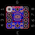
Attached is the simplified adapter PCB layout. I tied EN pin to VCC and GND pin to VEE and added 0805 size rail-to-rail decoupling cap. I tried to keep the loop area between output and inverting input traces small but it is not so easy with VSON10 and DIP8 pin assignment.
I have one more question. Is it OK to route the negative supply to the OPA1622 through the rail-to-rail decoupling capacitor pad as on the attached layout or it is better to also connect it to the thermal pad and thus shorten the VEE supply path?
Regards,
Oleg
Attachments
One thing I didn't mention was: I tried not to route anything between the DIP-8 rows and the edge of the board. So the adapter could be cut down to a smaller footprint to save some more space (e.g. in a mobile headphone amp).
But as I see, you don't think that seems necessary/worth the effort? ;-)
@agdr/all: I would order a batch of unpopulated boards, either by first setting up a GB or just offering them after I got them.
For assembled boards: The PCBs and caps are cheap, but 100 OPA1622 come at 550USD. For assembly I suspect something in the range of 100 USD, and the same amount for insured shipping to germany. Add about 20% german taxes [duty] on top of that and get at least 800 USD costs for 100 boards (more likely 1000USD).
Looking at OPA2134 prices at the german domestic retailers I suppose excess assembled boards could be commercially sold for about 20 to 30 USD each, so that might be interesting for some.
But being a student I don't want to handle that much value/take that much risk/get to know the deep details of european import duty & tax & warranty regulations.
If someone else wants to do that: Step up and feel free to take over
Last edited:
Well, making the adapter smaller (routing traces differently) is difficult without compromising the IC performance. The adapter layout that I propose can be made a bit smaller (by ~0.5 mm in each dimension) but the success of it largely depends on the production tolerances of the PCB fab where the adapters will be produced.
As for the GB, you are more or less right about the prices and overall investment needed. The next problem is keeping track of payments, actually packaging and shipping. One really has to invest a lot of time into it. Also don't forget to add some extra funds for managing "dead" or lost on delivery units etc. For me personally it is just too much trouble.
I'll post the gerbers here in a day or two when I finalize the layout.
I think I can write a quick webscript for the management stuffAs for the GB, you are more or less right about the prices and overall investment needed. The next problem is keeping track of payments, actually packaging and shipping. One really has to invest a lot of time into it. Also don't forget to add some extra funds for managing "dead" or lost on delivery units etc. For me personally it is just too much trouble.
Software is kind of my native domain. Packaging & shipping will likely be some effort (I have experience with sending some hundred DIN A4 letters), but I believe I can print labels or solve that otherwise...I'll post the gerbers here in a day or two when I finalize the layout.
Cool
After a busy week I have some free time today, so I'll also change my layout to include traces on the boards edge. That should really simplify some things. I am still wondering on tying Vee to GND. I see how that greatly simplifies things. And as I understood John, the performance should not degrade much. But I'd actually prefer a solution that's more versatile - even if that means putting two 0603 decoupling caps on the board.
For op-amp rolling a very simple variant would probably be best, but those doing some prototyping should also be able to use more of the ICs features.
With a two caps layout, the Vee-GND cap could be shorted by default.
Similar to EN, which could always be pulled 'high' for drop-in replacement, but with a cuttable trace so the user could put it in a prototyping circuit where he wants to use the EN feature of the IC.
- Status
- This old topic is closed. If you want to reopen this topic, contact a moderator using the "Report Post" button.
- Home
- Amplifiers
- Headphone Systems
- OPA1622/VSON10 breakout board layout