TI has recently made an evaluation board available for their nearly-unsolderable-by-hand OPA1622 headphone driver chip. The board goes for $25 via the TI website (direct ship from TI, Mouser doesn't stock it yet) for $25. I couldn't pass that up! So here are unboxing and hookup photos. I'm listening to it right now as I type this. Sounds excellent!
The website link at TI to buy one is here (the "order now" button at the right on the top banner):
OPA1622 Audio Operational Amplifier Evaluation Module - OPA1622EVM - TI Tool Folder
and the evaluation datasheet link is here (opens PDF)
http://www.ti.com/lit/ug/sbou172/sbou172.pdf
Photos:
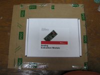
* The first 4467 shows the shipping box and the white box the eval module is packaged in. Lol that shipping box measures 15 x 15 x 2 inches. That is large corporation for "we can mail a box this size for the same price UPS charges you to mail a pack of gum"
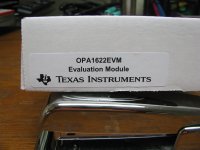
* 4469 is the ID sticker on the white box.
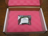
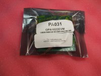
* 4470, 71, and 72 are opening the lid...
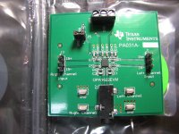
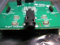
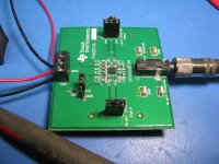
* 4473, 79, and 74 are front, back, and the 3.5mm output jack section of the board. Pretty slick on the output section, they have those connection rings for test clips and/or scope probes! Notice in 4479 the square patch of heat sink foil under the chip on the bottom of the board, connected thermally by those 4 vias under the chip. That has been one of my questions, did TI intend for the heat sinking to happen this way or via "wings" that stick out the sides on the top, which is what I've used on my boards.
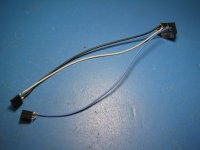
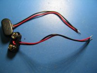
* 4475, and 4476 are getting the input connection wires ready. Those 3 pin header sockets that fit the board's input connectors are something I just happened to have on hand, Mouser #517-929974-01-03-RK. They are the same ones that fit the power connectors on Victor's low-THD oscillator board.
Notice that the input connectors on the evaluation board are set up for differential input, since they are marked in- and in+. I want to use single-ended, which is why I've bent the in- socket pin in photo 4475 to solder to the middle ground pin. And yes, that middle pin of the 3 is ground, I rung it out with the ohmmeter. TI has a minor screw-up there by not labelling those two middle pins. The single-ended input will then go between the in+ pin for each channel and the ground/in- pin, which is what the wiring in the next photo shows.
I'm using a Mouser #502-35RAPC2BV4 jack here (switchcraft 35RAPC2BV4) 3.5mm jack here. The terminal closest to the jack is ground, the next up is tip (left) and the next is ring (right).
I'm out of photo slots, so on to part 2....
Remember that you can zoom up any of these by clicking on those arrows in the bottom left corner.
The website link at TI to buy one is here (the "order now" button at the right on the top banner):
OPA1622 Audio Operational Amplifier Evaluation Module - OPA1622EVM - TI Tool Folder
and the evaluation datasheet link is here (opens PDF)
http://www.ti.com/lit/ug/sbou172/sbou172.pdf
Photos:
* The first 4467 shows the shipping box and the white box the eval module is packaged in. Lol that shipping box measures 15 x 15 x 2 inches. That is large corporation for "we can mail a box this size for the same price UPS charges you to mail a pack of gum"
* 4469 is the ID sticker on the white box.
* 4470, 71, and 72 are opening the lid...
* 4473, 79, and 74 are front, back, and the 3.5mm output jack section of the board. Pretty slick on the output section, they have those connection rings for test clips and/or scope probes! Notice in 4479 the square patch of heat sink foil under the chip on the bottom of the board, connected thermally by those 4 vias under the chip. That has been one of my questions, did TI intend for the heat sinking to happen this way or via "wings" that stick out the sides on the top, which is what I've used on my boards.
* 4475, and 4476 are getting the input connection wires ready. Those 3 pin header sockets that fit the board's input connectors are something I just happened to have on hand, Mouser #517-929974-01-03-RK. They are the same ones that fit the power connectors on Victor's low-THD oscillator board.
Notice that the input connectors on the evaluation board are set up for differential input, since they are marked in- and in+. I want to use single-ended, which is why I've bent the in- socket pin in photo 4475 to solder to the middle ground pin. And yes, that middle pin of the 3 is ground, I rung it out with the ohmmeter. TI has a minor screw-up there by not labelling those two middle pins. The single-ended input will then go between the in+ pin for each channel and the ground/in- pin, which is what the wiring in the next photo shows.
I'm using a Mouser #502-35RAPC2BV4 jack here (switchcraft 35RAPC2BV4) 3.5mm jack here. The terminal closest to the jack is ground, the next up is tip (left) and the next is ring (right).
I'm out of photo slots, so on to part 2....
Remember that you can zoom up any of these by clicking on those arrows in the bottom left corner.
Attachments
-
 IMG_4467.JPG481.9 KB · Views: 594
 -
 IMG_4469.JPG474.2 KB · Views: 565
 -
 IMG_4470.JPG442.5 KB · Views: 561
 -
 IMG_4471.JPG493.7 KB · Views: 563
 -
 IMG_4472.JPG484 KB · Views: 557
 -
 IMG_4473.JPG542.7 KB · Views: 262
 -
 IMG_4479.JPG469.4 KB · Views: 273
 -
 IMG_4476.JPG562 KB · Views: 195
 -
 IMG_4475.JPG631.3 KB · Views: 213
 -
 IMG_4474.JPG417 KB · Views: 213
Last edited:
TI OPA1622EVM headphone driver eval board unboxing and hookup, part 2
Continued from above...
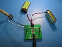
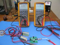
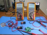
I'm going to use 9V batteries for now just because they are easy. These are actually 7.4V nominal "9V" lithium polymer rechargeables. I've measured the internal resistance on these in another thread to be around 0.3 ohms.
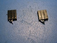
* 4480 shows the 9V battery snaps, Keystone 235-M.
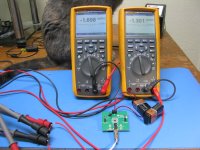
* 4485 shows it all hooked together and working! The chip is completely cool, but then again I'm using fairly high sensitivity 32R headphones.
When I first snapped in the batteries and had a listen I got nothing. Nada. Completely silent. Pondered it a bit and I seemed to remember from the OPA1622 datasheet that grounding the enable pin, that 2-pin jumper on the board near the power header, disabled the outputs. I pulled off the jumper and there was my music!
So now that it is working I read the instructions. The evaluation module pdf I linked in the post above has all sorts of useful information, including that bit about the enable pin. They do say in words that the middle pin of those input headers is ground, even if it isn't labeled on the board.
Finally, something interesting. Photos 4487 and 89 show an issue with the chip that is why I haven't used it in a project yet, along with the DIY soldering problem. The input bias current is a whopping 1.2uA. The chip really is intended to be fed by a balanced input from a DAC, where the impedance to ground on each input can be kept roughly equal to help zero out the input offset current IR drops. In single ended mode here the net result is around -1.5mV DC output offset (-1.7 on one channel and -1.3 on the other). Not bad, and still half the typical 3.3 mV of NwAvGuy's O2 headphone amplifier, but anymore I'm trying to keep that DC offset very low. In another thread I recently posted some photos of the OPA827 looped around and LME49600 producing 15uV! With proper differential inputs I'll bet the OPA1622 can also hit some mighty low DC output offset numbers.
Great sounding chip at any rate. I'll bet the OPA1622 becomes the "go to" chip for laptop, tablet and cell manufacturers who want to follow their DACs with a first rate headphone driver. The super tiny size is perfect for those devices. I think TI really has a commercial winner on their hands here, even if it may not be very DIY friendly.
Continued from above...
I'm going to use 9V batteries for now just because they are easy. These are actually 7.4V nominal "9V" lithium polymer rechargeables. I've measured the internal resistance on these in another thread to be around 0.3 ohms.
* 4480 shows the 9V battery snaps, Keystone 235-M.
* 4485 shows it all hooked together and working! The chip is completely cool, but then again I'm using fairly high sensitivity 32R headphones.
When I first snapped in the batteries and had a listen I got nothing. Nada. Completely silent. Pondered it a bit and I seemed to remember from the OPA1622 datasheet that grounding the enable pin, that 2-pin jumper on the board near the power header, disabled the outputs. I pulled off the jumper and there was my music!
So now that it is working I read the instructions.
The evaluation module pdf I linked in the post above has all sorts of useful information, including that bit about the enable pin. They do say in words that the middle pin of those input headers is ground, even if it isn't labeled on the board.Finally, something interesting. Photos 4487 and 89 show an issue with the chip that is why I haven't used it in a project yet, along with the DIY soldering problem. The input bias current is a whopping 1.2uA. The chip really is intended to be fed by a balanced input from a DAC, where the impedance to ground on each input can be kept roughly equal to help zero out the input offset current IR drops. In single ended mode here the net result is around -1.5mV DC output offset (-1.7 on one channel and -1.3 on the other). Not bad, and still half the typical 3.3 mV of NwAvGuy's O2 headphone amplifier, but anymore I'm trying to keep that DC offset very low. In another thread I recently posted some photos of the OPA827 looped around and LME49600 producing 15uV! With proper differential inputs I'll bet the OPA1622 can also hit some mighty low DC output offset numbers.
Great sounding chip at any rate. I'll bet the OPA1622 becomes the "go to" chip for laptop, tablet and cell manufacturers who want to follow their DACs with a first rate headphone driver. The super tiny size is perfect for those devices. I think TI really has a commercial winner on their hands here, even if it may not be very DIY friendly.
Attachments
Last edited:
What happens without one battery...
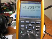
I ran out of edit time on the post above. One more thing, a word of caution for anyone messing with this evaluation board and using batteries. Here is what happens to the DC output if one of your battery snaps is loose, one of the thin battery snap wires breaks off at the binding post, or in the case of lithium cells like this the internal protection module decides it is going to do a low battery cutoff. 1.7Vdc applied to your headphones! Volt scale on the DMM here vs. mV scale in the posts above. So be sure to connect your batteries first, without the headphone plugged in, then plug in the headphone, which is what I did in my tests above.
This is why NwAvGuy has that power management circuit in his dual-battery O2 headamp and why I put something similar in my dual-battery Super CMOY project. If one battery "goes away" it is essential that both batteries get cut off instantly to protect the headphones. Pretty much any dual rail op-amp is going to put signficant DC on the output if one power rail goes away.
I ran out of edit time on the post above.
One more thing, a word of caution for anyone messing with this evaluation board and using batteries. Here is what happens to the DC output if one of your battery snaps is loose, one of the thin battery snap wires breaks off at the binding post, or in the case of lithium cells like this the internal protection module decides it is going to do a low battery cutoff. 1.7Vdc applied to your headphones! Volt scale on the DMM here vs. mV scale in the posts above. So be sure to connect your batteries first, without the headphone plugged in, then plug in the headphone, which is what I did in my tests above.This is why NwAvGuy has that power management circuit in his dual-battery O2 headamp and why I put something similar in my dual-battery Super CMOY project. If one battery "goes away" it is essential that both batteries get cut off instantly to protect the headphones. Pretty much any dual rail op-amp is going to put signficant DC on the output if one power rail goes away.
Attachments
Last edited:
Instead of leaving the -ve input pin floating, try grounding it. A solder blob on the header should do the trick.
That is exactly what the bent pins on the input sockets are doing.
They ground out the v- pin to the center ground pin. But you may be thinking about the v+ pin on the test with the one battery removed. I just noticed the part of the photo that shows the other end of the input cable is cut off. For that test I unplugged the cable from the input source, which did result in the v+ input floating (v- grounded). To see if that made a difference I tried shorting across the input connector pins with a screwdriver, to ground the v+ pin, but no change in the 1.7V DC output.
Attachments

Last edited:
Have you ensured that the offset is not coming from the source? What's it like with both inputs grounded? What is your source resistance? Instead of shorting the -ve input to ground, can you try grounding it with a resistor of equal value?That is exactly what the bent pins on the input sockets are doing.
(I would be using shielded cables for the inputs, but that's probably just me.)
OlegSh has a nice design for the 1622 here. http://www.diyaudio.com/forums/headphone-systems/290801-universal-buffer-headamp-based-opa1622.html
Maybe you could try those regulators if you decide to go mains powered instead of battery.
Have you ensured that the offset is not coming from the source? What's it like with both inputs grounded? What is your source resistance? Instead of shorting the -ve input to ground, can you try grounding it with a resistor of equal value?
(I would be using shielded cables for the inputs, but that's probably just me.)
OlegSh has a nice design for the 1622 here. http://www.diyaudio.com/forums/headphone-systems/290801-universal-buffer-headamp-based-opa1622.html
Maybe you could try those regulators if you decide to go mains powered instead of battery.
Yep the source doesn't have any DC - capacitor coupled. The evaluation board schematic shows a 1K to ground and another 1K in series with the non-inverting input.
By way of comparison the NJM2068 used in the O2 headphone amp gain stage has a 150nA input bias current. Then there is the OPA1688 headphone driver I'm using in another project with FET inputs and pA input bias current.
OlegSh is doing a good job with his board! I've left a few thoughts in his thread. I believe he posted a few months ago he was looking at looping another chip around the OPA1622 to solve the input bias current problem - I suggested the OPA827 - but I haven't had a chance to circle back recently and see where he is at now. A looped pair like that would require some stability analysis. Great layout job he is doing though, IMHO.
My goal with this thread is just the unboxing and quick test of this OPA1622 evaluation module. At just $25 it was too good to pass up.
Last edited:
Can you try leaving the -ve input floating (maybe put a capacitor there to reduce noise pickup)?
You never told me what the offset was like with both inputs grounded. Output capacitors sometimes leak.
Planning on getting one of these myself. Thanks for all the detailed info.
You never told me what the offset was like with both inputs grounded. Output capacitors sometimes leak.
Planning on getting one of these myself. Thanks for all the detailed info.
correction: 61uV and 317uV DC output with both inputs grounded!
SamAnytime -
The DC output tests I did above were with the eval board input unplugged from the source, the other end of that grey 3.5mm cable. So the source DC or impedance actually doesn't matter here. I forgot about that in my previous post.
BUT - it is good you've asked the question, because it turns out my shorting the floating V+ input to ground with a screwdriver in post #2 didn't make contact somehow. I've re-done the test here with a more solid soldered shorted pin for the V+.
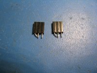
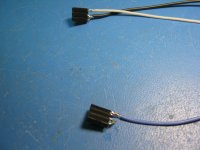
* photo 4520 (mouse over the photos for the number) shows the shorting input socket. I just took the socket used in the posts above, removed the wires, and bent/soldered the V+ pin the same as the V- pin to the middle grounded pin.
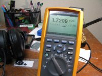
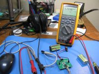
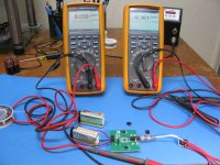
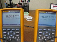
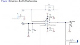
* photos 4521, 23, and 24 show the test setup. The fully-grounded input sockets are now installed. I've switched to primary 9V batteries here. 4524 shows the result: 61 microvolts on one channel and -317 microvolts on the other! No complaints from me about that. The ground return path on the eval board - schematic below - is about the same on each channel, so that large 1uA input bias current is more-or-less cancels out.
* photo 4525 is the same test with both inputs shorted, but back to the lithium polymer rechargeable cells. Same result.
* photo 4526 shows the results with both input sockets removed now, such that both inputs are floating on both channels. Result: 33uV and 161uV. But the inputs are not really floating. Per the schematic below the eval board includes ground return resistors on each channel.
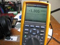
* photo 4531 & 32 now show just the v- input shorted, but the v+ left floating, which is back to test test I did in post #2 when I unplugged the source cable. And back to the same result I had previously: -1.7mV and -1.3mV.
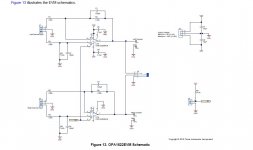
Finally here is the board schematic from the evaluation datasheet which shows why all this is happening.
In the final case, with the v- input grounded and v+ floating, One end of R1 gets grounded which results in the stage reverting to a standard non-invertinng op amp with a gain of 2x. With v+ left floating R3 is diconnected and the non-inverting input is returned to ground through the 1K R4.
So looking back out the non-inverting pin it is 1K impedance. 1K * 1uA = 1mV. Looking out the inverting pin it is the two 1K in parallel, 500 ohms, so 500 * 1uA = .5mV. The difference between the two for DC input offset is then 0.5mv, and add that to the inherent chip input offset of 100uV gives 0.6uV. Then gain that up by the stage gain of 2x gives 2 * 0.6 = 1.2mV. Q.E.D.
Fast Eddie D - The board includes a 3.5mm output jack, but just the 3 pins on each channel for input. That $25 includes shipping! No tax either. Whatever TI is paying in shipping for that huge box is included in the $25.
Sergey888 - thanks for the info!
SamAnytime -
The DC output tests I did above were with the eval board input unplugged from the source, the other end of that grey 3.5mm cable. So the source DC or impedance actually doesn't matter here. I forgot about that in my previous post.
BUT - it is good you've asked the question, because it turns out my shorting the floating V+ input to ground with a screwdriver in post #2 didn't make contact somehow.
I've re-done the test here with a more solid soldered shorted pin for the V+.* photo 4520 (mouse over the photos for the number) shows the shorting input socket. I just took the socket used in the posts above, removed the wires, and bent/soldered the V+ pin the same as the V- pin to the middle grounded pin.
* photos 4521, 23, and 24 show the test setup. The fully-grounded input sockets are now installed. I've switched to primary 9V batteries here. 4524 shows the result: 61 microvolts on one channel and -317 microvolts on the other!
No complaints from me about that. The ground return path on the eval board - schematic below - is about the same on each channel, so that large 1uA input bias current is more-or-less cancels out.* photo 4525 is the same test with both inputs shorted, but back to the lithium polymer rechargeable cells. Same result.
* photo 4526 shows the results with both input sockets removed now, such that both inputs are floating on both channels. Result: 33uV and 161uV. But the inputs are not really floating. Per the schematic below the eval board includes ground return resistors on each channel.
* photo 4531 & 32 now show just the v- input shorted, but the v+ left floating, which is back to test test I did in post #2 when I unplugged the source cable. And back to the same result I had previously: -1.7mV and -1.3mV.
Finally here is the board schematic from the evaluation datasheet which shows why all this is happening.
In the final case, with the v- input grounded and v+ floating, One end of R1 gets grounded which results in the stage reverting to a standard non-invertinng op amp with a gain of 2x. With v+ left floating R3 is diconnected and the non-inverting input is returned to ground through the 1K R4.
So looking back out the non-inverting pin it is 1K impedance. 1K * 1uA = 1mV. Looking out the inverting pin it is the two 1K in parallel, 500 ohms, so 500 * 1uA = .5mV. The difference between the two for DC input offset is then 0.5mv, and add that to the inherent chip input offset of 100uV gives 0.6uV. Then gain that up by the stage gain of 2x gives 2 * 0.6 = 1.2mV. Q.E.D.
Fast Eddie D - The board includes a 3.5mm output jack, but just the 3 pins on each channel for input. That $25 includes shipping! No tax either. Whatever TI is paying in shipping for that huge box is included in the $25.
Sergey888 - thanks for the info!
Attachments
-
 opa1622EVM.JPG50.5 KB · Views: 176
 -
 IMG_4532.JPG588.4 KB · Views: 105
 -
 IMG_4531.JPG714.5 KB · Views: 85
 -
 IMG_4526.JPG612 KB · Views: 86
 -
 IMG_4525.JPG612.1 KB · Views: 290
 -
 IMG_4524.JPG527.5 KB · Views: 296
 -
 IMG_4523.JPG560.5 KB · Views: 297
 -
 IMG_4521.JPG568.9 KB · Views: 300
 -
 IMG_4520.JPG342.3 KB · Views: 307
 -
 opa1622evm2.JPG42.7 KB · Views: 144
Last edited:
Exactly. So I think the best would be to leave the -ve input floating (or put a capacitor there to reduce noise pickup). This gives you the DC result in photo 4526.In the final case, with the v- input grounded and v+ floating, One end of R1 gets grounded which results in the stage reverting to a standard non-invertinng op amp with a gain of 2x. With v+ left floating R3 is diconnected and the non-inverting input is returned to ground through the 1K R4.
So looking back out the non-inverting pin it is 1K impedance. 1K * 1uA = 1mV. Looking out the inverting pin it is the two 1K in parallel, 500 ohms, so 500 * 1uA = .5mV. The difference between the two for DC input offset is then 0.5mv, and add that to the inherent chip input offset of 100uV gives 0.6uV. Then gain that up by the stage gain of 2x gives 2 * 0.6 = 1.2mV. Q.E.D.
Okay, so if someone like myself would like to try this board, what needs to be done with the inverting input in order to use plain ole' unbalanced inputs without excessive offset?
I'll bet that in general most folks would consider that existing 1.2mV-or-so to be low. I know NwAvGuy did, he considered the 3mV out of his O2 headamp to be "low". Lol, I disagreed.
I've also had email and PM chats with folks over the years who wonder why it even matters. My view is a very low offset, like under 200uV or so, keeps the drivers in sensitive IEMs and headphones close to their natural mechanical idle position during signal zero crossings, ie average motion. But a case can be made as to whether that is even an audible difference.So I'm probably just being excessively picky!
But for the excessively picky like me I think this thing really needs a low-offset buffer in front of it, preferably with FET inputs. I just took a look at the latest posts in OlegSh's thread and it does look like he is pursuing the buffer.But long story short, I would say by all means get this eval board and give it a try! The OP1622 sounds just fantastic and that 1.2mV DC won't harm anything. This board is a good, cheap, way to get a listen to that hard-to-solder part. Then keep following OlegSh's thread for his final product, which should be pretty good!
Last edited:
Have you tested your TI evaluation board?
Hello SamAnytime,
Thanks for posting.
I was checking out the TI OPA1622 evaluation board User’s Guide. The input impedance looks to be 1K ohms to match the output impedance of the upstream DAC output impedance of 500R ohms. 1K ohms is not the typical headphone input impedance. What are you test driving this thing with?
I am playing with A LME49600 headphone buffer. TI’s evaluation board is an order of magnitude higher than $25. I went to ebay and bought a few PCB’s. Then I went to Sparkfun.com and bought a hot air tool and solder paste.
Reflow solder is not that difficult with the hot air tool. (to my susprize)
I am connecting the first attempt at hot air reflow solder to the audio analyzer this weekend.
Have you tested your TI evaluation board?
DT
So I'm probably just being excessively picky!
Nothing wrong with that. The 1.2mV offset doesn't bother me. I would like to try it as a preamp, not as a headphone amp.
Is it best to ground R3 and R5 so as to use it as a non-inverting amplifier with a gain of 2?
Oops!
agdr, it was you I meant to thank for for posting this thread.
DT
Good questions!
The OPA1622 eval board should be 2K input Z on the non-inverting board input - R3 + R4 - and probably 2K on the inverting board input, although I would need to think about that inverting a bit more.
2K is a curious choice for input impedance. The thinking there may have been that a lot of "audio" spec'ed op amps seems to be rated down to a 2K load, like the NJM2068. I used an LME49990 based unity-gain buffer I had sitting around, between an ODAC and the input of the eval board. I believe that George once wrote the ODAC won't be happy (slight THD increase, if I'm remembering right) below a 10K load (the O2 headamp's input Z). The 49990 is rated down to a 600R load. Then I had an old ODA board of mine with just the 12 4.7uF Wima film caps soldered on, 6 in parallel on each channel, and used that as coupling. The resulting 28uF combined with that 2K input should put the corner frequency somewhere around 2.8Hz.
I'll admit to being out-of-date on what is out there for DACs these days, but I would guess 1K would be quite a load for a DAC too. If anyone knows please post! Maybe a 1K balanced load is what today's DACs are expecting.
Yeah that LME49600 eval board will break the bank! I've never bought one for that reason. Interesting about the hot air soldering. I *really* need to give that a try. I have a hot air station I bought a couple of months ago just sitting here, but haven't have time to try it out yet.
I have done any THD+N tests on this eval board and probably won't because it looks like they have done some Audio Precsion tests in the data sheet. I just have a "toy" QA401 distortion tester.
Is it best to ground R3 and R5 so as to use it as a non-inverting amplifier with a gain of 2?
In this writeup I'm making sure to distinguish between the board's inverting input and the chip's, same with the non-inverting side of things.
Sergey888 and SamAnytime probably have the best solution there, a capacitor (bank) from the eval board's inverting input (pin 3 of the board's J1 and J3) on the board datasheet to ground. Then the same capacitor value from the non-inverting input (pin 1 on J1 and J3) to the source.
At DC that capacitor from the board inverting input to ground will be open, taking R1 and R5 out of the circuit, and leaving r2 and r6 as the input Z the chip inverting pins sees, just 1K now. That also is a unity gain config, so no gain-up either.
Then at DC with that blocking capacitor between the source and the board pin 1R3 and R7 will be taken out of the circuit, leaving just R4 and R8 as the non-inverting input Z, also 1K. So net result is 1K on each input, everything cancels but the chip's inherent 100uV or so, multiplied by the stage 1x gain at DC.
Then with AC in the audio range that cap from inverting board input to ground would be around 114 ohms at 50Hz and less at higher frequencies, so effectively just back to the "nearly grounded" R1 & R5 for the AC stage gain of 2.
Then at the board non-inverting input the coupling cap is the same 114R at 50Hz, less at higher F, putting R3 & R7 back in the circuit. So net result is now 2K Z on each chip input and back to balanced cancellation. Just the 100uV chip offset, now times the 2x stage gain.
For the coupling cap and cap on the inverting input, something similar to the six 4.7uF 50Vdc Wima film caps in parallel that I'm using would work.
Interesting circuit!
Having a capacitor from the inverting input resistor to ground on non-inverting stages has been around a long time. I just never even given using that configuration a second thought anymore because it historically required an electrolytic to get C values big enough for the audio range. And then the circuit leaves the chip's inherent input DC offset, which has usually been large itself. So instead I would go with a DC servo setup or injecting current into one input, which is how I did the DC cancellation on the ODA amplifier.BUT... things have apparently changed! The film caps have value large enough these days that using a bunch of them in parallel is an option. In fact, I think there are single 30uF or so film caps in stock at Mouser, I just couldn't use them on the ODA board due to size limitations. Then on the chip offset side of things, these inherent input DC offsets are extremely low now, as with the OPA1622 here, so if you can cancel out the input IR drops with the capacitors the remaining chip inherent input DC offset is no big deal, even gained-up.
Hey a big thanks to Sergey888 and SamAnytime for the comments!
Last edited:
Methods to measure the immeasurable
Hello,
This is likely old news to some.
Speaking of distortion testing, in the old days of Burr Brown prior to the merger with Texas Instruments, Burr Brown developed methods to measure distortion below the ability of the Audio Precision analyzers they had on the bench at the time. Texas instruments continues to use these methods to measure the immeasurable today.
One of the Burr Brown methods goes like this; the (DUT) is an active part of the test circuit. The signal generator connects to the + input of the op-amp under test. 100% of the DUT output is feed back to the – input of the DUT. With 100% negative feedback all of the test frequency and all of the distortion of the function generator is canceled out, the only thing that remains is the error or DUT distortion. This error signal is too low to be processed by the AP analyzer’s DAC’s. The error signal is amplified to a level that that can be processed by the AP DAC’s. This test method adds 10 to 15 db’s to the capabilities of the audio analyzer.
DT
- Status
- This old topic is closed. If you want to reopen this topic, contact a moderator using the "Report Post" button.
- Home
- Amplifiers
- Headphone Systems
- TI OPA1622EVM headphone driver eval board unboxing and hookup, part 1