More on the battery internal resistance measurements above. I'm just excited about that lithium polymer result, but I shouldn't be unnecessarily spooking people about the throw-away 9V batteries or "9V" NiMH batteries. They will work just fine, even with 16R headphones. ")
The situation is the same as using an unregulated power supply with a CRC filter in an AC powered amp, where the 5.7 ohms or 2.2 ohms is the resistor between caps in the CRC. The net result is the maximum output swing of the amplifier will just be reduced a bit by the voltage drop across the battery internal resistance.
For example, with a total of 15mA through the battery from both channels, that 5.7 ohms internal resistance in the 9V primary cells would cause a power rail drop of just 5.7R * 15mA = 90mVdc on each rail. With both channels at the maximum 75mA, the power supply rail drop would be 5.7R * 150mA = 0.86Vdc on each rail.
Also a note on why I chose (around) 60mA as the test current. That puts the discharge rate at 0.25C for the 250mAhr Tenegy 9V NiMH, 0.2C for the Powerex 9V NiMH, and just 0.08C for the 740mAhr lithium polymer, all moderate discharge rates well under 1C. 60mA would be 30mA per channel, about half the OPA1688 maximum.
Last edited:
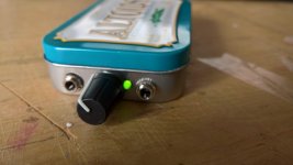
Yes the knob is a bit too big if mounted with the board parts touching the bottom on the altoids can. But I have done that not even thinking and it slightly touches but doesnt seem to cause any real issue. So I could get another can OR just put some small "feet" on the bottom of the can!! Voila!!
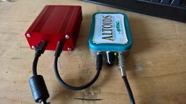
Here are some pix with the led on:
Also note I have the headphones and dac plugged into the wrong jacks!!! LOL.
Listening to the amp outside on the enclosure then flipping it upside down makes this an easy mistake to do!! No Sound!! LOL!
Working ok fine so far and sounds great!
Alex
Note does anyone have a smaller know that would fit and look good? Maybe a smaller diamter silver metal knob??
Attachments
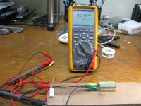
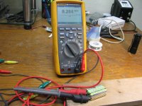
Lithium 9V battery internal resistance at a 0.25C discharge rate
I wanted to see if the internal resistance of the lithium polymer "9V" battery was current dependent (non-linear) by trying a heavier load. Turns out it isn't! Still essentially the same.
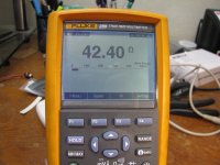
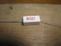
In the photos below the new load resistor is a 43 ohm 5W "sand" type, measuring at 42.40 ohms, which gives a discharge rate of 0.25C (around 185mA) for the 740mAhr battery. The lithium battery has been recharged after the test yesterday. 0.25C is the dicharge rate used for the NiMH "9" cells above, giving a better apples-to-apples comparison between "9V" NiMH and "9V" lithium polymer.
The open circuit voltage is 8.28Vdc, the voltage under load is 8.21Vdc. The current through the series setup is 8.21/42.40 = 194mA, close to 0.25C. The voltage across the internal battery resistance is 8.28 - 8.21 = 0.07Vdc.The internal resistance of this rechargeable battery is then 0.07Vdc/194mA = 0.361 ohms, compared with 0.381 ohms above for the 0.08C discharge rate. Fairly consistent. At the 0.25C discharge rate the battery is dumping 8.21Vdc^2 / 42.40R = 1.6 watts into the resistor.
I wanted to see if the internal resistance of the lithium polymer "9V" battery was current dependent (non-linear) by trying a heavier load. Turns out it isn't! Still essentially the same.
In the photos below the new load resistor is a 43 ohm 5W "sand" type, measuring at 42.40 ohms, which gives a discharge rate of 0.25C (around 185mA) for the 740mAhr battery. The lithium battery has been recharged after the test yesterday. 0.25C is the dicharge rate used for the NiMH "9" cells above, giving a better apples-to-apples comparison between "9V" NiMH and "9V" lithium polymer.
The open circuit voltage is 8.28Vdc, the voltage under load is 8.21Vdc. The current through the series setup is 8.21/42.40 = 194mA, close to 0.25C. The voltage across the internal battery resistance is 8.28 - 8.21 = 0.07Vdc.The internal resistance of this rechargeable battery is then 0.07Vdc/194mA = 0.361 ohms, compared with 0.381 ohms above for the 0.08C discharge rate. Fairly consistent. At the 0.25C discharge rate the battery is dumping 8.21Vdc^2 / 42.40R = 1.6 watts into the resistor.
Attachments
Last edited:
Another unscientific observation, with the lower impedance cans I have <100 Ohms contrasted with the Beyer T90's 250 ohms the volume knob with the T90s have to be cranked up a bit more to make them come alive. still more than enough power can not listen sanely with the knob turned up all the way. <100 Ohms volume is set between 11 o'clock and 12 o'clock, the T90s vol is 12 o'clock to 2pm.
Alex
Alex
Revised front panel hole template, new knobs
Excellent suggestion!! I've been thinking about it since I read your post. I think you are 100% correct. That slim rubberized knob I had specified in the BOM is just the wrong thing for the CMOY. It needs a smaller knob. So the problem isn't raising the PC board 2mm to fit that knob, the problem is finding a slimmer knob. Having the board sit on the 3.5mm jacks is just fine, as I originally intended.
So for knobs, here is a start. Adafruit has some T18 shaft slim knobs that are 10 mm in diameter, in either 10 mm long or 15 mm long:
https://www.adafruit.com/products/2058
https://www.adafruit.com/products/2057
I've just ordered some to try out. If they work I'll have them available on the sales thread, so folks won't have to place a separate order.
The mechanical measurements for the Super CMOY show 5.8mm of space from the center line of the pot shaft to the mint tin bottom, if the board is sitting upside down on the 3.5mm jacks, plus an additional 0.2mm for the bottom metal thickness. That is a total of 6.0mm from the pot shaft to table top, so any knob less than 6.0 x 2 = 12.0 mm should clear the table. The 10mm knobs here should work great. The slim rubberized knobs I had listed previously are 13.2 mm in diameter, just 1mm too much.
And... below and out at the Google Drive link is a revised version of the front panel hole template. This one is back to the Super CMOY sitting upside down on the 3.5mm jacks. The hole template now includes an optional 2mm hole for the LED light to come through, with the LED soldered in the rear position that clears the panel.
Thanks for the suggestion, Alex!
Note does anyone have a smaller know that would fit and look good? Maybe a smaller diamter silver metal knob??
Excellent suggestion!! I've been thinking about it since I read your post. I think you are 100% correct. That slim rubberized knob I had specified in the BOM is just the wrong thing for the CMOY. It needs a smaller knob. So the problem isn't raising the PC board 2mm to fit that knob, the problem is finding a slimmer knob. Having the board sit on the 3.5mm jacks is just fine, as I originally intended.
So for knobs, here is a start.
Adafruit has some T18 shaft slim knobs that are 10 mm in diameter, in either 10 mm long or 15 mm long:https://www.adafruit.com/products/2058
https://www.adafruit.com/products/2057
I've just ordered some to try out. If they work I'll have them available on the sales thread, so folks won't have to place a separate order.
The mechanical measurements for the Super CMOY show 5.8mm of space from the center line of the pot shaft to the mint tin bottom, if the board is sitting upside down on the 3.5mm jacks, plus an additional 0.2mm for the bottom metal thickness. That is a total of 6.0mm from the pot shaft to table top, so any knob less than 6.0 x 2 = 12.0 mm should clear the table. The 10mm knobs here should work great. The slim rubberized knobs I had listed previously are 13.2 mm in diameter, just 1mm too much.
And... below and out at the Google Drive link is a revised version of the front panel hole template. This one is back to the Super CMOY sitting upside down on the 3.5mm jacks. The hole template now includes an optional 2mm hole for the LED light to come through, with the LED soldered in the rear position that clears the panel.
Thanks for the suggestion, Alex!
Attachments
Last edited:
Jet Lag + Coffee (LOTS  ) + Long Flight Delay in Beijing = A Neat Idea?
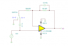
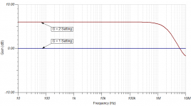
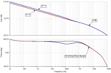
So I did a quick stability simulation on the G = 1 configuration and a 400pF load and I wasn't really happy with the result (about 25 degrees of phase margin if I remember correctly). The problem is that in a gain of 1, the inverse feedback factor (1/feedback factor, the inverse of quantity of the output signal that is fed back to the input) is already 0dB, so I can't really create a dip in the curve to get a boost in phase margin. BUT I can increase the inverse feedback factor without actually changing the signal gain, this technique for stabilization is commonly called noise gain (because...well...it increases the noise). The trick is to only increase the inverse feedback factor outside of the audio bandwidth, so we still have the low noise and distortion of the gain = 1 configuration at the frequencies we care about. And at high frequency, near the loop closure point I have some extra inverse feedback factor and can use my little 47pF capacitor to boost phase margin.
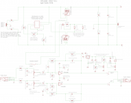
But enough control theory, the circuit is attached. It uses a switch to select between G = 1 and G = 2. You could also do this with a jumper and have many selectable gains. The phase margin with a 400pF capacitive load for both G = 1 and G = 2 is 50 degrees (loop gain and phase plot is attached). Also attached is the frequency response in both settings so you can see that the signal gain is exactly what you would expect. This might be a good way to may a CMoy more flexible to accommodate multiple headphone types.
) + Long Flight Delay in Beijing = A Neat Idea?So I did a quick stability simulation on the G = 1 configuration and a 400pF load and I wasn't really happy with the result (about 25 degrees of phase margin if I remember correctly). The problem is that in a gain of 1, the inverse feedback factor (1/feedback factor, the inverse of quantity of the output signal that is fed back to the input) is already 0dB, so I can't really create a dip in the curve to get a boost in phase margin. BUT I can increase the inverse feedback factor without actually changing the signal gain, this technique for stabilization is commonly called noise gain (because...well...it increases the noise). The trick is to only increase the inverse feedback factor outside of the audio bandwidth, so we still have the low noise and distortion of the gain = 1 configuration at the frequencies we care about. And at high frequency, near the loop closure point I have some extra inverse feedback factor and can use my little 47pF capacitor to boost phase margin.
But enough control theory, the circuit is attached. It uses a switch to select between G = 1 and G = 2. You could also do this with a jumper and have many selectable gains. The phase margin with a 400pF capacitive load for both G = 1 and G = 2 is 50 degrees (loop gain and phase plot is attached). Also attached is the frequency response in both settings so you can see that the signal gain is exactly what you would expect. This might be a good way to may a CMoy more flexible to accommodate multiple headphone types.
Attachments
It is worth to mention that opamp open loop output impedance is somewhat current dependent. This is especially noticeable for lower power opamps, when output stage has a quite low bias current. In such case output impedance has an obvious peak when output current is around 0, and in this region opamps are more sensitive to a capacitive load.
Opamp models, unless they are made on transistors level, do not represent these effects, and as a result they do not give a full picture of what is going to happen in such case with a real device.
OPA1688 has a moderate GBW, which helps, but it is still quite a low power device and it is worth to keep an eye on this.
If you run into a problem like that, it is not too hard to fix it by lowering the crossover frequency even more by adding RC in between opamp inputs. Similar way to what John did, but without affecting overall gain (you can also make it smarter combining it with an input filter, but it works only for an inverting amp). Or just by adding an output RC damping.
NB Also a signal source is not always an ideal voltage source, may affect results somewhat.
Last edited:
The phase margin with a 400pF capacitive load for both G = 1 and G = 2 is 50 degrees (loop gain and phase plot is attached).
johnc124 - Outstanding! Thank you for taking the time to work through this! Much appreciated. Your solution to increase the unity gain phase margin makes perfect sense. I agree, 25 degrees is getting thin enough that sooner or later somebody out there with a long cable and just the right headphones may have oscillated.
The timing is great, I have nealry run out of PC boards from the first fabrication run. I was about to send out a V4.1 with a few cosmetic changes, but no functional changes - until now!
Luckily I have space for the two new 0.1nF 50V C0G MLCC caps, C13 and C14 below. I also have the layout and schematic posted in a new V4.1 folder out on the Google Drive link.For the gain of 1x, the new C13 and C14 are populated. For gains of 2x, 3x, or 4x C13 and C14 are left out, with the capacitor pad that connects to the resistor (R9, R8) is jumpered to ground. For C14 that is the new JP4 ground pad next to the cap pad to jumper. For C13 the bottom pad of the capacitor just solders to the right end of R6 (which is ground) with a piece of jumper wire.
For folks who already have the V4.0 boards I'll be posting some simple re-work instructions in a "rework" folder at the Google Drive link to add the two 0.001uF caps. For the rework I'm going to specify axial 1nF C0G caps to make the rework easy. No need to do any rework unless you want to use 1x unity votlage gain rather than the 2x, 3x, or 4x in the BOM.
Lucien - excellent question you asked there!
Sergey888 - thanks for the input! If that effect shows up in the testing now we will know why. Good point about the ideal voltage (signal) source. In fact, I think johnc124 wrote in the vendor thread that he specified a non-ideal (SMPS) model for the rail voltage sources when they did design on the OPA1622 to make sure it was real-world proof!
Attachments
Last edited:
That's correct. While designing the OPA1622 I required that all distortion simulations be performed with at least a 3 ohm power supply impedance. At first my design team didn't care about the requirement, but it eventually drove many of the design decision for that product (just take a look at the PSRR).
Hold on, guys! Saying "signal source" I didn't mean supply sources. I know that the way I construct sentences is a bit odd, but not to that extend
When freq compensation is performed by adding an impedance in between inputs, you result will depend on other impedances connected to the inputs, including you signal source. It is unlikely will cause a big problem, but you have to check corner use cases, like no source connected etc.
Also, while having lower valuer resistors values in feedback is beneficial from an output noise point of view, it barely will do any improvement in case like this. I would keep resistor values a bit higher than ~800Ohms, so you can use a higher impedance RC for compensation. Just remember about an input capacitance, that is it.
Lucien - excellent question you asked there!
Don't mention it. I figure I have just enough knowledge to be dangerous, while not quite accomplishing anything.
I think I need to download TINA and have a play. Have not touched loop stability in... uh... years, so this should be... "interesting".
Also, I think I'll aim for ~1.25x gain with that 47 pF compensation cap. Will let you know if I accomplish anything useful.
When freq compensation is performed by adding an impedance in between inputs, you result will depend on other impedances connected to the inputs, including you signal source. It is unlikely will cause a big problem, but you have to check corner use cases, like no source connected etc.
Hey Sergey888! Your wording was just fine, I did understand that you meant the signal source impedance. That just happened to remind me of what johnc124 had written about his efforts with the power supply voltage sourcel models.
You have a good point! Like you say, anytime a reactive element is introduced any others connected can have an effect. It would be interesting to do some more sims on that 1nF cap addition with a typical line level impedance added to the signal source voltage source. In this case, from the point where the 1nF is added to the non-inverting input, working back to the amp input, there is the 49.9K ground return resistor, the 3.3uF coupling cap (which should affect anything here), then the (10K) pot wiper, and finally the 274R input resistance that form the RF filter with the 220pF to ground, then the source impedance. Other than source impedance, out of all that I suspect the RF filter would be the thing that might have an effect.
And speaking of sims...
I may go with this against local traditions, but would recommend to start with LTSpice. Yes, it looks a bit less user friendly, however it is much more powerful instrument, in my opinion. Also there is a huge online community which can help with pretty much any question.
I completely agree here, I don't like TINA a bit. Worse, the TI version is essentially freeware that wants the user to upgrade to the (paid) manufacturers version for the more important functions, as I recall. LTSpice is the way to go. For anyone using the Eagle layout editor out there, LTSpice is now part of Eagle too. You can move the schematic between the two.
Also, I think I'll aim for ~1.25x gain with that 47 pF compensation cap. Will let you know if I accomplish anything useful.
I like your thoughts of using the 1.25x! That seems like a good compromise on it all. Please do post how that works out.
Also, while having lower valuer resistors values in feedback is beneficial from an output noise point of view, it barely will do any improvement in case like this. I would keep resistor values a bit higher than ~800Ohms, so you can use a higher impedance RC for compensation. Just remember about an input capacitance, that is it.
I forgot to comment here!
Another standard set of values folks can try is 1K for the feedback resistor and ground resistor for 2x gain, 1K + 499R for 3x, 1K + 332R for 4x, 1K + 249R for 5x, and 1K + 200R for 6. Mouser has 1/8W-sized resistors in stock for all of these values.Move that LED
The discussion on moving the LED was over several pages ago, I'm just now getting up to speed on the thread.
I use a clip-ring mount shown here:
http://www.mouser.com/ProductDetail/Bivar/CR-104/?qs=sGAEpiMZZMsVdjGoHXLeS4GGdrOe1EGe550EWP5qpJc=
BIVAR makes them in both 3mm and 5mm size (3mm size in the link). I think the possibly make square ones, but not at all sure about that though.
They are super cheap, look super good, can be installed/removed numerous times. One caveat: the hole has to be the right size.
I first saw them in a digital project in mid-80's. And they're still around!
I use a clip-ring mount shown here:
http://www.mouser.com/ProductDetail/Bivar/CR-104/?qs=sGAEpiMZZMsVdjGoHXLeS4GGdrOe1EGe550EWP5qpJc=
Nice solution! It looks like those are just 5mm deep vs. 12mm for the type I posted. 12mm is getting pretty long for the small mint tin.
Quick Question
I have a quick question..... I will probably be making a custom case and wondering if there would be any impact (noise, etc.) in: instead of soldering the battery connector wires directly to the PCB, soldering 4 pin right angle headers to the PCB and connecting the batteries with a 4 pin JR connector to make it easier to remove/replace batteries?
Just running ideas while I design the case..... thoughts appreciated.
KD
A battery header is OK! In fact I sized those 4 holes for a 0.1" header and originally intended to use one, so the battery clips could just be plugged onto the header. That would make the battery wires a bit more break-proof too if the insulation had some support in a header socket. The problem though is all the headers I could find were too tall when the socket was plugged in. I thought about trying a right angle, but it seemd like it would hit the batteries. If you are able to make a header fit, please post some pictures!
Also, something I've been meaning to post in general, might as well twist the two battery clip wires together for each snap. The whole thing is in a metal mint tin so EMI pickup is likely to be nil, but might as well twist the wires anyway.
Last edited:
- Home
- Amplifiers
- Headphone Systems
- OPA1688 Super CMOY, 2x 9V with real ground and headphone relay - PCBs