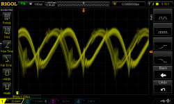
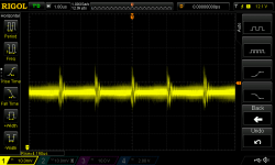
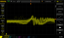
I remeasured the DC-DC converter output ripple. Following the suggestion of AIM65 I discovered that my previous measurements were mostly pickup noise and not the true output of the DC-DC converter. In the attached waveforms the first one is the input which comes from the AC-DC adapter (USB charger) measured at the end of 50cm long USB cable connected to the loaded DC-DC converter. I get similar waveform when using the USB power bank instead of the charger. The second is the DC-DC converter output waveform measured on its pins. The third is the output zoom-in. As can be seen there are spikes on both input and output every 2.2 us followed by the ringing at around 100MHz with around 10mV amplitude which quickly decays (see zoom-in of the output waveform). According to Jim Williams these spikes can be reduced by using ferrite beads and I guess T or Pi filters tuned to 100MHz. Other than these spikes there are no other visible problems with the output voltage. So now is the time to order some ferrite beads and RF filters and try this converter with the headamp.
Attachments
Last edited:
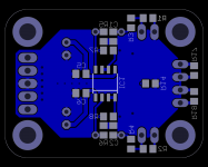
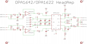
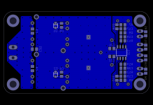
I am still perfecting my OPA1622/OPA1642 headphone amp design. I've added DC blocking capacitor pads (5mm pin pitch) and removed a couple of unnecessary resistors.
Attachments
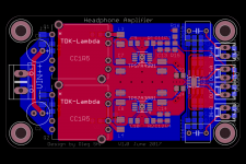
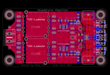
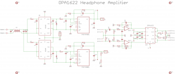
I decided to try a complete headamp solution using a pair of low power 5V DC-DC converters. Ideally it would be best to use just one bipolar type but TDK-Lambda bipolar converters with +-5V outputs do not exist. Attached are the schematic and PCB layout I am going to try. All inductors are 1kOhm@100MHz ferrite beads. All 1210 (imperial) size ceramic capacitors are 22uF 25V type. Electrolytic caps at the input are there for reducing the supply ripple and associated EMI. I plan to use 47uF capacitors there since USB charger may not like higher capacitance.
Attachments
Thanks for the comments, JP!
I'll "stitch" the planes together with more vias, this is easy") Regarding more copper I guess you mean the top layer. I can probably just copy the bottom layer pour to the top layer.
Regarding more copper I guess you mean the top layer. I can probably just copy the bottom layer pour to the top layer.
As for the cap from primary to secondary I've added one on the PSU board using similar DC-DC converter in the other thread but got the comment that capacitive coupling between primary and secondary should be avoided. I guess I'll follow what you and datasheet suggest and will add the cap as an option. Chassis ground is the other story. I plan to connect the GND to chassis at the headphone jack (just by using nonisolated socket) so I think extra connection is not necessary. In addition I'll probably provide the GND pad between the regs which can be connected straight to chassis.
I'll "stitch" the planes together with more vias, this is easy
Regarding more copper I guess you mean the top layer. I can probably just copy the bottom layer pour to the top layer. As for the cap from primary to secondary I've added one on the PSU board using similar DC-DC converter in the other thread but got the comment that capacitive coupling between primary and secondary should be avoided. I guess I'll follow what you and datasheet suggest and will add the cap as an option. Chassis ground is the other story. I plan to connect the GND to chassis at the headphone jack (just by using nonisolated socket) so I think extra connection is not necessary. In addition I'll probably provide the GND pad between the regs which can be connected straight to chassis.
Updated design
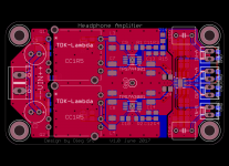
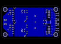
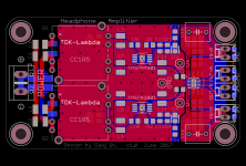
Used more copper and more vias as suggested. Schematic is almost the same except for the added GND pin and capacitor from primary (negative terminal) to secondary common (GND).
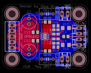
Board's size is 4x7cm.
Used more copper and more vias as suggested. Schematic is almost the same except for the added GND pin and capacitor from primary (negative terminal) to secondary common (GND).
Board's size is 4x7cm.
Attachments
Last edited:
Würde mich freuen!
TDK Lambda CC1R5 3D STEP/IGS downloaded.
Working on same idea but with an expensive 8W GAIA converter (using them excessively in airborne developments and therefore I´m lucky with samples; really good support for the price): 24VDC out of 2S LiFePO4 18650 pack for portable headphone amplifier based on Pete Millett´s NuHybrid headphone amplifier. Pending for the moment while trying to finish 211 amplifier (never ending story).
Waiting for your finalized design.
Have a nice sunday.
JP
Thanks! I usually take a day or two off before finalizing the design. It helps to look at it with the fresh eye to see if something is not ideal
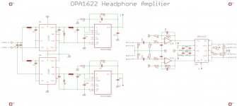
Regarding the design itself, my idea was to design a small but high performance and not too expensive headphone amp. The OPA1622 in my other implementation performs superb and so I decided to give it a try with not too expensive DC-DC converter supply. Lets see how it will perform in such a configuration.
Regarding the design itself, my idea was to design a small but high performance and not too expensive headphone amp. The OPA1622 in my other implementation performs superb and so I decided to give it a try with not too expensive DC-DC converter supply. Lets see how it will perform in such a configuration.
One more update
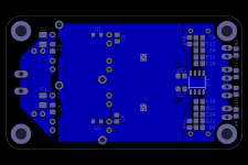
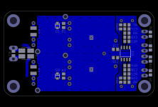
Following the discussion in my DC-DC converter based power supply design thread I've added common mode choke to the power entry side. Updated schematic and PCB layout are attached.
Following the discussion in my DC-DC converter based power supply design thread I've added common mode choke to the power entry side. Updated schematic and PCB layout are attached.
Attachments
3D views
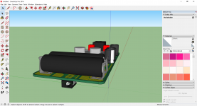
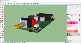
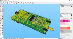
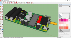
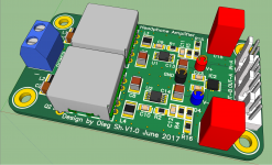
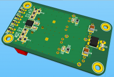
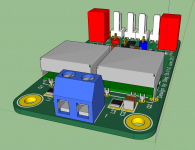
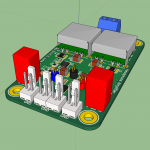
JPS64 has kindly provided 3D renderings of the design (see attached). Now it is time to produce the PCBs, assemble the headamp and try it
JPS64 has kindly provided 3D renderings of the design (see attached). Now it is time to produce the PCBs, assemble the headamp and try it
Attachments
In case you can still modify the schematics, I would recommend to add some protection shottky diodes to the output of the TPS7Axxxx power supply.
I had a design, when a TPS7A4700 and a TPS7A3001 provided a dual PSU for a bunch of opamps, and in case the negative supply comes up first for some reason, it could falsify the output of the positive supply through some internal diodes of the opamps, and pull the output of the TPS7A4700 positive supply well below 0V, near to the negative supply! (what the TPS7A4700 could not regulate out, and started to became hot as far as I remember)
Adding some clamping shottkys to the output of the regulators (both positive and negative): it does not allow the positive supply to be pulled lower than 0V than the Vf of the shottky: and this way the positive supply was able to regulate to the required value.
[hint came from TI]
Good point, meszarosa. I fitted protection diodes on my PSU PCB based on TPS7A4901 and TPS7A3001 pair. The reason to omit them here is that there is no excessive capacitance preceding the regs and thus turn off is more or less instant while start up is controlled by the RC network which has the same time constant for both regs and thus has to be simultaneous. I thought that it should prevent polarity reversal but I will add the diodes pads just in case. Thanks for reminder.
- Status
- This old topic is closed. If you want to reopen this topic, contact a moderator using the "Report Post" button.
- Home
- Amplifiers
- Headphone Systems
- Universal buffer/headamp based on OPA1622