EDIT: 5/19/2017
I just realized that I never posted the Google Drive link to all the Inverting O2 Project materials! Here it is:
https://drive.google.com/drive/folders/0B67cJELZW-i8S1VmUzZsUGZZN00?usp=sharingZZN00?usp=sharing
then the V3.61 folder. That contains the schematic, layout, bill of materials, build instructions, etc.
The original first post is below.
*************************************************************************************
Have you ever wondered what the result would have been if NwAvGuy had used inverting amplifier stages for the gain and output sections of his O2 Headphone Amplifier rather than non-inverting? Well wonder no more.
I've put together an inverting O2 version over the last few months and finally had a chance to run some THD+N tests on it vs. the original NwAvGuy O2. What I've expected would happen is cancellation of the higher-order even harmonics by the inverting stages at a cost of slightly higher background noise. The additional noise is due to the higher value of gain resistors (10K, 24.9K) required by an inverting amplifier (Johhnson noise and current noise). The input impedance is still 10K, but with an inverting amplifier that 10K is in series with the input. With a non-inverting amplifier it is from the input to ground, as in the orignal O2, with just 274 ohms or so in series for the RF filter.
Well, sure enough, that is exactly what happens! The plots below show some AC powerline noise leaking in via the fluorescent room lighting, which makes a good input test signal. The 4th harmonic at 240Hz is gone, as is the 6th at 360Hz, etc. The overall background noise has increased by about 10dB it appears. The gain chip in this one is a FET-input LME49880 which helps mitigate some current noise, as does the output stage which is a FET-input OPA2140 wrapped around BUF634s, set up as an inverting amp. I've also used the Vishay RN50C series 1/8W resistors throughout to lower current noise a bit.
Although this is the general format of the O2 headamp with (now inverting) gain stage feeding a pot in the middle (5K here for some reduced noise) and the (now inverting) output stage, it looks like that same overall design was patented at one point in 1984 using inverting stages for exactly the same reason, even harmonic cancellation:
https://www.google.com/patents/US4628278
Lol, I *think* that patent has expired, it has been more than 20 years, but I'll check further. The patent was from John Fluke Manufacturing, the DMM people.
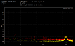
* The first plot below shows a 10KHz test signal into the inverting version of the O2. The even harmonics at 240Hz (4th), 360Hz (6th), and 480Hz (8th) are gone but the noise floor is about 10dB higher than the stock O2 below.
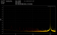
* The second plot shows a 10KHz test signal into a standard O2 headamp. This one is built up exactly from NwAvGuy's BOM, no modifications or part substitutions of any kind. It is running on batteries for this test with no AC adaptor plugged in.
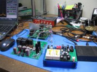
* The first photo shows the test setup. Signal generator output (one of Victor's low THD oscillators) BNC T'ed into a QA400 tester and then into one channel the DUT's input, either an O2 or the inverting O2 here.
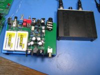
* The second photos shows the two O2s. The inverting version is about an inch wider than the standard O2. Fits into the blue B5-080 case. The black one is the standard O2 in a B2-080 case.
I just realized that I never posted the Google Drive link to all the Inverting O2 Project materials! Here it is:
https://drive.google.com/drive/folders/0B67cJELZW-i8S1VmUzZsUGZZN00?usp=sharingZZN00?usp=sharing
then the V3.61 folder. That contains the schematic, layout, bill of materials, build instructions, etc.
The original first post is below.
*************************************************************************************
Have you ever wondered what the result would have been if NwAvGuy had used inverting amplifier stages for the gain and output sections of his O2 Headphone Amplifier rather than non-inverting? Well wonder no more.
I've put together an inverting O2 version over the last few months and finally had a chance to run some THD+N tests on it vs. the original NwAvGuy O2. What I've expected would happen is cancellation of the higher-order even harmonics by the inverting stages at a cost of slightly higher background noise. The additional noise is due to the higher value of gain resistors (10K, 24.9K) required by an inverting amplifier (Johhnson noise and current noise). The input impedance is still 10K, but with an inverting amplifier that 10K is in series with the input. With a non-inverting amplifier it is from the input to ground, as in the orignal O2, with just 274 ohms or so in series for the RF filter.
Well, sure enough, that is exactly what happens! The plots below show some AC powerline noise leaking in via the fluorescent room lighting, which makes a good input test signal. The 4th harmonic at 240Hz is gone, as is the 6th at 360Hz, etc. The overall background noise has increased by about 10dB it appears. The gain chip in this one is a FET-input LME49880 which helps mitigate some current noise, as does the output stage which is a FET-input OPA2140 wrapped around BUF634s, set up as an inverting amp. I've also used the Vishay RN50C series 1/8W resistors throughout to lower current noise a bit.
Although this is the general format of the O2 headamp with (now inverting) gain stage feeding a pot in the middle (5K here for some reduced noise) and the (now inverting) output stage, it looks like that same overall design was patented at one point in 1984 using inverting stages for exactly the same reason, even harmonic cancellation:
https://www.google.com/patents/US4628278
Lol, I *think* that patent has expired, it has been more than 20 years, but I'll check further. The patent was from John Fluke Manufacturing, the DMM people.
* The first plot below shows a 10KHz test signal into the inverting version of the O2. The even harmonics at 240Hz (4th), 360Hz (6th), and 480Hz (8th) are gone but the noise floor is about 10dB higher than the stock O2 below.
* The second plot shows a 10KHz test signal into a standard O2 headamp. This one is built up exactly from NwAvGuy's BOM, no modifications or part substitutions of any kind. It is running on batteries for this test with no AC adaptor plugged in.
* The first photo shows the test setup. Signal generator output (one of Victor's low THD oscillators) BNC T'ed into a QA400 tester and then into one channel the DUT's input, either an O2 or the inverting O2 here.
* The second photos shows the two O2s. The inverting version is about an inch wider than the standard O2. Fits into the blue B5-080 case. The black one is the standard O2 in a B2-080 case.
Attachments
-
 10KHz Victor osc into inverting O2 red_is_out 3.png50.6 KB · Views: 2,053
 -
 10KHz Victor osc into standard O2 red_is_out 3.png50.1 KB · Views: 2,017
 -
 IMG_3586.JPG82.2 KB · Views: 2,014
 -
 IMG_3587.JPG65.1 KB · Views: 2,043
 -
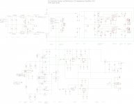 inverting O2 schematic.jpg459.5 KB · Views: 2,219
 -
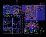 inverting O2 layout.jpg992.8 KB · Views: 1,226
Last edited:
...Great job agdr.
I think I read a thread some time back here on diyaudio that inverting amps has a proven better performance, but I can't find anything.
Since I am also doing some experimenting with inverted vs noninverted amplifier circuits, I want to investigate the theory about this a little deeper...can you point me in a direction?
...and now the important question:How does it sound compared to the original?
Nrik - thanks! I really haven't found a lot out there via Google searching on inverting amps.
One of the big benefits is elimination of common-mode distortion since both op-amp inputs stay at zero volts with respect to ground. sgrossklass did an excellent post about that in a thread months ago, or maybe even was last year, but I probably couldn't find it now.
And it sounds great! I'm still trying to determine if I can actually hear any audible difference vs. the standard O2 though. Goes back to NwAvGuy's "sighted bias" comments. To do it right I really should set up a blind A/B test sometime.
I really haven't found a lot out there via Google searching on inverting amps. One of the big benefits is elimination of common-mode distortion since both op-amp inputs stay at zero volts with respect to ground. sgrossklass did an excellent post about that in a thread months ago, or maybe even was last year, but I probably couldn't find it now.
And it sounds great!
I'm still trying to determine if I can actually hear any audible difference vs. the standard O2 though. Goes back to NwAvGuy's "sighted bias" comments. To do it right I really should set up a blind A/B test sometime.jcx - thanks for the confirm on the patent lifespan.
Yeah just the overall topology is simlar to the O2. The gain stage followed by the pot in the middle followed by unity gain (-1 in this case) current buffer output stage (I spotted a typo on the print, that should be a 24.9K feedback resistor in the output stage for unity gain), two NiMH rechargeable batteries with a power management circuit to cut then off when low, a voltage doubler power supply simiar to the O2 (I've used heat sinked LDOs here though), and fits into a similar case.
But it is different enough that it probably wouldn't be considered a "derivative" as per the O2's license. I've come to learn that for the "derivative" test to hold a circuit apparently has to be extemely similar. Plus he disappeared years ago and is non-contactable. I'm told that in several countries that alone is enough for a license to revert to the public domain (non contactable for more than 1 year).
I'll post the Gerber files once it is done and tested, probably a couple of months from now, if anyone wants to build one. The photos are V2.0 but the schematic is a V3.0 that is still being fiddled with. George's ODAC fits in the battery area in place of the batteries too, same as the O2. V3.0 has an input select switch the ODAC can be sent through.
Although the FET-input chips help with current noise they have higher voltage noise than bipolar, of course. I want to try building one up with (bipolar) OPA1612 chips instead and see where the noise floor lands.
Yeah just the overall topology is simlar to the O2. The gain stage followed by the pot in the middle followed by unity gain (-1 in this case) current buffer output stage (I spotted a typo on the print, that should be a 24.9K feedback resistor in the output stage for unity gain), two NiMH rechargeable batteries with a power management circuit to cut then off when low, a voltage doubler power supply simiar to the O2 (I've used heat sinked LDOs here though), and fits into a similar case.
But it is different enough that it probably wouldn't be considered a "derivative" as per the O2's license. I've come to learn that for the "derivative" test to hold a circuit apparently has to be extemely similar. Plus he disappeared years ago and is non-contactable. I'm told that in several countries that alone is enough for a license to revert to the public domain (non contactable for more than 1 year).
I'll post the Gerber files once it is done and tested, probably a couple of months from now, if anyone wants to build one. The photos are V2.0 but the schematic is a V3.0 that is still being fiddled with.
George's ODAC fits in the battery area in place of the batteries too, same as the O2. V3.0 has an input select switch the ODAC can be sent through.Although the FET-input chips help with current noise they have higher voltage noise than bipolar, of course. I want to try building one up with (bipolar) OPA1612 chips instead and see where the noise floor lands.
Last edited:
How exciting agdr! I saw the article on your web a while ago, then it disappeared! Happy to see you kept working on that.
I guess we'll all have to practice surface mount soldering!
Opamp rolling will be a bit trickier too... but WTH?!
Seriously, do you have any estimates about price, bare board or with just the surface mount components already soldered?
I guess we'll all have to practice surface mount soldering!
Opamp rolling will be a bit trickier too... but WTH?!
Seriously, do you have any estimates about price, bare board or with just the surface mount components already soldered?
Hi guys!
Yep if anyone should be interested in this amp once I get the final version tested I'll sell the PC board at-cost to forum members, plus I'll post the Gerbers if anyone wants to fab their own board. I mainly did this one for fun, just out of curiousity wanting to hear what two inverting stages would sound like.
Way back when, a month or so after the O2 was released, I asked NwAvGuy via PM if he had considered inverting stages for the O2 headamp. Since the O2 has two stages it works out especially well, you wind up with two inversions = non-inverting output. I can't remember his his exact reply now, but he had thought about it.
The total parts price so far on the BOM looks like about $70 at Mouser, not including the transformer and case. The parts for the low-battery cutoff power management circuit can be left off on this one if not using batteries, which saves some money. The new per-battery PM circuit uses a couple of new-generation optical solid state relay chips (just 0.015 ohms "on", 1/20th of the O2's mosfets!) that are $6 each at Mouser, so that is $12 of the $70 right there.
I've debated a bit whether to even post this amp, given all the controversy over NwAvGuy's license. Lol, adydula has been good enough to listen to some of my rantings on the issue via email over the last couple of months. I was glad to see jcx' posting. If folks can't even really see a correlation to the O2 that is great news in terms of the amp not being a "derivative"!
The whole amp is largely through-hole, except the power management circuit. On this amp the PM circuit is *only* for the batteries, to cut them off when low. The AC power doesn't go through it at all. This amp has a separate headphone relay, like my O2 Booster Board, to take care of thumps. NwAvGuy tried to make his PM circuit do both low battery cutoff and thump elimination. In my view it didn't quite succeed well at either.
So if you are not using batteries then all those power management surface mount parts (the stuff under the PCB under the batteries on the layout) can be left off. The other surface mount parts are the two op-amps (all the op-amps "better" than the NJM2068 are surface mount, it seems), two transistors under the board for current sources for the on/off LEDs, and 2.2uF caps across the .22uF film caps. Those latter 2.2's could also be done as through hole parts under the board though.
I "corrected" a bunch of things about the O2 that had been bugging me ever since it was released. All the good stuff from the O2 Booster Board is rolled into the amp too. I used BUF634's as the output current buffers rather than LME49600's because they come in TO-220 and I can (and do) heat sink them.
Yep if anyone should be interested in this amp once I get the final version tested I'll sell the PC board at-cost to forum members, plus I'll post the Gerbers if anyone wants to fab their own board. I mainly did this one for fun, just out of curiousity wanting to hear what two inverting stages would sound like.
Way back when, a month or so after the O2 was released, I asked NwAvGuy via PM if he had considered inverting stages for the O2 headamp. Since the O2 has two stages it works out especially well, you wind up with two inversions = non-inverting output. I can't remember his his exact reply now, but he had thought about it.
The total parts price so far on the BOM looks like about $70 at Mouser, not including the transformer and case. The parts for the low-battery cutoff power management circuit can be left off on this one if not using batteries, which saves some money. The new per-battery PM circuit uses a couple of new-generation optical solid state relay chips (just 0.015 ohms "on", 1/20th of the O2's mosfets!) that are $6 each at Mouser, so that is $12 of the $70 right there.
I've debated a bit whether to even post this amp, given all the controversy over NwAvGuy's license. Lol, adydula has been good enough to listen to some of my rantings on the issue via email over the last couple of months. I was glad to see jcx' posting. If folks can't even really see a correlation to the O2 that is great news in terms of the amp not being a "derivative"!
The whole amp is largely through-hole, except the power management circuit. On this amp the PM circuit is *only* for the batteries, to cut them off when low. The AC power doesn't go through it at all. This amp has a separate headphone relay, like my O2 Booster Board, to take care of thumps. NwAvGuy tried to make his PM circuit do both low battery cutoff and thump elimination. In my view it didn't quite succeed well at either.
So if you are not using batteries then all those power management surface mount parts (the stuff under the PCB under the batteries on the layout) can be left off. The other surface mount parts are the two op-amps (all the op-amps "better" than the NJM2068 are surface mount, it seems), two transistors under the board for current sources for the on/off LEDs, and 2.2uF caps across the .22uF film caps. Those latter 2.2's could also be done as through hole parts under the board though.
I "corrected" a bunch of things about the O2 that had been bugging me ever since it was released.
All the good stuff from the O2 Booster Board is rolled into the amp too. I used BUF634's as the output current buffers rather than LME49600's because they come in TO-220 and I can (and do) heat sink them.
Last edited:
Yep, go for it agdr
I remember testing things regarding the low battery problem. Never got it solved though. The obvious solution came from you agdr - oda with more parts.
Regarding the non-inverting vs inverting versions I expect not to hear any difference unless you decide to change the sonic signature. The performance has gone beyond what is hearable... Which reminds me of control over the gain at different frequensies... Still at the top of life at 55 I suppose it is showing that I take planning for the future seriously ...
Regards
I remember testing things regarding the low battery problem. Never got it solved though. The obvious solution came from you agdr - oda with more parts
.Regarding the non-inverting vs inverting versions I expect not to hear any difference unless you decide to change the sonic signature. The performance has gone beyond what is hearable... Which reminds me of control over the gain at different frequensies
... Still at the top of life at 55 I suppose it is showing that I take planning for the future seriously ...Regards
Absolutely great news!!!
I am glad you published this.... in the spirit of " I wonder if...." LOL!!
This is one amp that I would build just to listen to it in comparison to the original O2 and ODA.
Also would like to listen to it in comparison to my fairly new BH Crack, which is a tube amp full of THD!
Alex
I am glad you published this.... in the spirit of " I wonder if...." LOL!!
This is one amp that I would build just to listen to it in comparison to the original O2 and ODA.
Also would like to listen to it in comparison to my fairly new BH Crack, which is a tube amp full of THD!
Alex
Listened the previous night to my very original O2 and it struck me - damn how good it sounds . Well, I will not put the oda in place before I decide on the knobs... Risk is that I will be handling raw pots ever after... 15-17mm diam/20mm lenght. AL with red line or small red LED (might maybe do this one myself as I have bought two old Unimat lathes). I will turn them into one CNC lathe and one CNC mill. But as I need the knobs earlier - please give me ideas on what would work with the dimensions stated .
Regards
. Well, I will not put the oda in place before I decide on the knobs... Risk is that I will be handling raw pots ever after... 15-17mm diam/20mm lenght. AL with red line or small red LED (might maybe do this one myself as I have bought two old Unimat lathes). I will turn them into one CNC lathe and one CNC mill. But as I need the knobs earlier - please give me ideas on what would work with the dimensions stated .Regards
Also would like to listen to it in comparison to my fairly new BH Crack, which is a tube amp full of THD!
I would be *extremely* interested in how it compares sonically to the Crack! One of the reasons I've used FET-input op amps is to better match the characteristics of tubes. The success of the Crack amp just goes to show that in the end "lowest THD" and "lowest noise" may not be what sounds the best to some folks' ears.
BTW, thanks for all the feedback on the amp over the last few months! Alex is the main reason why this one wound up with the front panel 1/4" jack, rear RCA jacks, and in the B5-080 case. I had it designed to fit the B3-080 case, the taller version of the O2, and to put an ODAC in the top slot along with the batteries. But Alex has convinced me that most folks are using their O2's as desktop amps. So this one is like the O2 in that the ODAC replaces the batteries. I posted a poll about it a few weeks ago. Last I looked it was like 5:1 desktop vs. portable.
There is still some space on the PC board over by the RCA jack. I'm thinking of adding another op-amp unity gain buffer to buffer the output of the ODAC on its way out the RCA jacks, if someone wants to wire up their RCAs that way. With the buffer the RCA cable capacitance won't load down the ODAC output. I'm also going to have to notch out that corner of the board and use panel-mounted RCA jacks. The one on the board in the photo was a test for spacing.
Which reminds me - this one will need front and back panels drilled and etched, so two panels to buy from Front Panel Express vs. just the one in the O2.
Turbon - good points! Yeah with this one there actually is a chance, no matter how small, that it could sound different from the O2 due to the inverting stages lowering common mode rejection error and even harmonics. Which reminds me, back on Nrik's question, here is a short one-page tech paper from Analog Devices on common mode rejection ratio in op-amps:
http://www.analog.com/media/en/training-seminars/tutorials/MT-042.pdf (opens PDF)
At the bottom of page 1 it says "Note inverting mode operating op amps will have less CMRR error. Since both inputs are held at a ground (or virtual ground), there is no CM dynamic voltage." One op-amp input is tied to ground and the other is held at zero volts WRT ground by the action of the op-amp feedback. CMRR is also why I tied the non-inverting input to ground through a resistor rather than directly, to make the impedance looking back out that pin as similar as possible to the one looking out the inverting input.
Now whether any of this is audible is something else entirely. Like you say, NwAvGuy's O2 Headamp's numbers are already most likely below the range of anyone's hearing. But who knows. I'm still just 50% on measurements. In the end I personally think the "how it sounds" part has to be rolled in there too, hence all the postive comments the Crack amp receives, as per Alex's post.
Lol, that revised power management circuit was a bit of a trick. I posted a thread about it in the power supply forum a month or two ago. Ever since he released the O2 I've thought it needed separate comparators on each battery. I can easily come up with a situation that would "fool" the O2's PM circuit into thinking the batts were OK when they are not. If one batt was fully charged to 10.15V (1.45V per cell) while the other battery was shorted and just producing 4.35V (I've had TWO of those Tenergy batteries do this!) the total would be 14.5, above the 14.0V PM threshold on the O2, and it would remain on. The new circuit checks each battery individually to make sure it is above 7.0V. Then I added my latch circuit to each to make sure it doesn't motorboat when the battery is low, like the O2 often does.
But it adds quite a pile of parts. one comparator on each battery, plus a transistor circuit to "wire AND" the two comparator outputs, then the optical SSDs to control the power flow from the batteries. I put the whole thing under the battery area as SMD parts, since the comparators involved are SMD. SMD 0.1% resistors for the sampling voltage divider are cheaper than 0.1% through hole. I really like the fact that in the new arrangement the AC power doesn't go through the PM circuit, or SSRs, at all, That stuff is now only on the batteries. I'll bet one of the circuit wizards here on the forum can come up with some slick way to acheive the same per-battery PM function with half the number of parts!
http://www.analog.com/media/en/training-seminars/tutorials/MT-042.pdf (opens PDF)
At the bottom of page 1 it says "Note inverting mode operating op amps will have less CMRR error. Since both inputs are held at a ground (or virtual ground), there is no CM dynamic voltage." One op-amp input is tied to ground and the other is held at zero volts WRT ground by the action of the op-amp feedback. CMRR is also why I tied the non-inverting input to ground through a resistor rather than directly, to make the impedance looking back out that pin as similar as possible to the one looking out the inverting input.
Now whether any of this is audible is something else entirely.
Like you say, NwAvGuy's O2 Headamp's numbers are already most likely below the range of anyone's hearing. But who knows. I'm still just 50% on measurements. In the end I personally think the "how it sounds" part has to be rolled in there too, hence all the postive comments the Crack amp receives, as per Alex's post.Lol, that revised power management circuit was a bit of a trick. I posted a thread about it in the power supply forum a month or two ago. Ever since he released the O2 I've thought it needed separate comparators on each battery. I can easily come up with a situation that would "fool" the O2's PM circuit into thinking the batts were OK when they are not. If one batt was fully charged to 10.15V (1.45V per cell) while the other battery was shorted and just producing 4.35V (I've had TWO of those Tenergy batteries do this!) the total would be 14.5, above the 14.0V PM threshold on the O2, and it would remain on. The new circuit checks each battery individually to make sure it is above 7.0V. Then I added my latch circuit to each to make sure it doesn't motorboat when the battery is low, like the O2 often does.
But it adds quite a pile of parts. one comparator on each battery, plus a transistor circuit to "wire AND" the two comparator outputs, then the optical SSDs to control the power flow from the batteries. I put the whole thing under the battery area as SMD parts, since the comparators involved are SMD. SMD 0.1% resistors for the sampling voltage divider are cheaper than 0.1% through hole. I really like the fact that in the new arrangement the AC power doesn't go through the PM circuit, or SSRs, at all, That stuff is now only on the batteries. I'll bet one of the circuit wizards here on the forum can come up with some slick way to acheive the same per-battery PM function with half the number of parts!
Last edited:
Cool idea. I can't say I'd have heard about LME49880 and OPA2140 before, but you live and learn...
The configuration that I'd find most interesting would be an inverting (or twice inverting if you value your absolute phase) input stage with a non-inverting buffer.
You know what I'd be most interested in as far as measurements of the stock O2 go? Distortion at 2 Vrms input for 2.5x gain, or generally shortly before clipping. High and only input-dependent levels in the gain stage are the concept's Achilles heel in practical use, and I bet a number of people who ended up disliking the amp were accidentally clipping theirs. The 6.5x gain setting in particular is further impeded by somewhat pathetic output driving in the NJM2068, as load impedance ends up around 1k5 then.
(Well, and it won't be the ideal amp for some HE-6s or other power-hungry planars. It would certainly be interesting to see what it does at 5 Vrms into 50 ohms or so.)
There's a reason why other 2-stage amps tend to have some gain in the output stage, like 8+/-2 dB. That makes it much harder to clip them on the input side while still keeping noise to reasonable levels.
I completely agree that folks clipping their O2s without realizing it has likely been the source of some bad reviews. The O2 topology pretty muich demands having a clipping detector in there, which I did with the ODA but was going to leave off on this one since the O2 didn't have one. Hmmm, I should re-think thiat. Maybe I can whip one up with fewer parts. Seems that I've seen several window comparators on-a-chip.
Good obverservation about the NJM2068 outout. I had noticed that, the datasheet specifies a maximum 2K load, which likely means they knew the THD would get worse past that point, especially with larger swings. In the new amp here the LME49880 is THD rated down to 600R, just like the LME49990. The feedback resistors have to be huge due to the inverting topology, so that pretty much leaves just the pot for load, which I've downsized to 5K to reduce Johnson noise. I would have gone to 1K like in the ODA, but I would have dissipation concerns with the dual package. In the ODA I have one separate LME49990 per channel for more dissipation.
Yeah I didn't know about the OPA140/2140 series either, I learned about that one from Sergey888 when designing the O2 booster board. I've found one interesting potential hiccup with the chip though. The open loop output impedance graph (fig 19 in the datasheet) kind of goes nuts below 1KHz (zooms up from 10R to 1K). Which would be less of a problem with the chip in a direct feedback loop, but I'm still pondering the effect with it driving a buffer (the BUF634 here or the LME49600 in my O2 booster board) since the loop is around both parts. I *think* the net outcome will be that it doesn't matter given the high input Z of the current buffer. I'll have to do some frequency response tests of that pair of parts. This particular issue is why I've gone to recommending the OPA827 in the booster board. The 827 shows low open loop output Z through the entire audio band (datasheet figure 27), completely flat in fact.
Hey excellent thoughts about having some gain in the output stage. Sold! I'll do it. In this one it will just mean upping the value of the buffer loop feedback resistor.
I wanted to implement this 13 year old comment from Nelson Pass about throwing some closed loop gain away to keep the op-amp further way from the unity gain stability point. Seems to make a lot of sense. But I just can't figure out how to implement it for the life of me. That is what the 10K resistors to ground on the inverting inputs were originally for, to form a voltage divider, but then later realized that is a zero volt point. A voltage divider isn't going to work, at least not without an input cap and the signal ground being different than the system ground. Then even later I relized that 10K to ground does have to be in there anyway to handle the case when nothing is plugging into the input - an input bias current return path to ground. I'm sure it is like looking at an elephant through a magnifying glass, the implementation of Nelson's comment is probably obvious, but it has me stumped. That whole thread is about how inverting op-amps sound and is pretty interesting - the first post is here.
Good obverservation about the NJM2068 outout. I had noticed that, the datasheet specifies a maximum 2K load, which likely means they knew the THD would get worse past that point, especially with larger swings. In the new amp here the LME49880 is THD rated down to 600R, just like the LME49990. The feedback resistors have to be huge due to the inverting topology, so that pretty much leaves just the pot for load, which I've downsized to 5K to reduce Johnson noise. I would have gone to 1K like in the ODA, but I would have dissipation concerns with the dual package. In the ODA I have one separate LME49990 per channel for more dissipation.
Yeah I didn't know about the OPA140/2140 series either, I learned about that one from Sergey888 when designing the O2 booster board. I've found one interesting potential hiccup with the chip though. The open loop output impedance graph (fig 19 in the datasheet) kind of goes nuts below 1KHz (zooms up from 10R to 1K). Which would be less of a problem with the chip in a direct feedback loop, but I'm still pondering the effect with it driving a buffer (the BUF634 here or the LME49600 in my O2 booster board) since the loop is around both parts. I *think* the net outcome will be that it doesn't matter given the high input Z of the current buffer. I'll have to do some frequency response tests of that pair of parts. This particular issue is why I've gone to recommending the OPA827 in the booster board. The 827 shows low open loop output Z through the entire audio band (datasheet figure 27), completely flat in fact.
Hey excellent thoughts about having some gain in the output stage. Sold!
I'll do it. In this one it will just mean upping the value of the buffer loop feedback resistor.I wanted to implement this 13 year old comment from Nelson Pass about throwing some closed loop gain away to keep the op-amp further way from the unity gain stability point. Seems to make a lot of sense. But I just can't figure out how to implement it for the life of me. That is what the 10K resistors to ground on the inverting inputs were originally for, to form a voltage divider, but then later realized that is a zero volt point. A voltage divider isn't going to work, at least not without an input cap and the signal ground being different than the system ground. Then even later I relized that 10K to ground does have to be in there anyway to handle the case when nothing is plugging into the input - an input bias current return path to ground. I'm sure it is like looking at an elephant through a magnifying glass, the implementation of Nelson's comment is probably obvious, but it has me stumped.
That whole thread is about how inverting op-amps sound and is pretty interesting - the first post is here.
Last edited:
Hmmm - after thinking about what I just wrote above about the 10K resistors from the inverting inputs to ground, that isn't correct. The op-amp (inverting) input bias current will still flow through the feedback resistor if there is no input. In fact, with no input, the inverting stage turns into a unity gain buffer with the input grounded.
So those 10K resistors to ground I have on the various inverting inputs are doing absolutely nothing and can be eliminated. Good, that is 4 less parts.
So those 10K resistors to ground I have on the various inverting inputs are doing absolutely nothing and can be eliminated. Good, that is 4 less parts.
Last edited:
Oops - RF filter
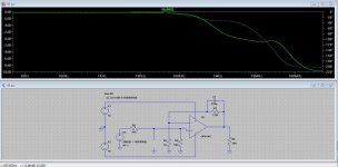
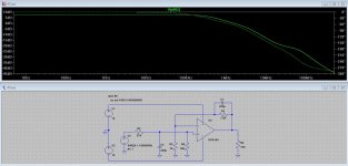
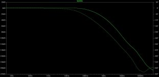
I've just realized that the input RF filters in this amp will suffer the same fate as the 10K resistors to ground on the inverting input in the post above. Things are a bit different with inverting amps.
The simple fix is to split the input 10K resistor into two 4.99K resistors with the RF filter capacitor between them, rather than at the inverting op amp input. The corner frequency winds up around 640KHz, vs. the 2.6MHz corner with the O2's RF filter.
I've used the OPA140 in the sims below since I've yet to find a LME49880 Spice model.
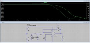
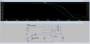
* The first plot is the result of an inverting -1 unity gain stage just with the low pass filter formed by the cap across the feedback resistor. Does a reasonable job through the 11MHz bandwidth of the op-amp, but the maximum rejection is around 60dB.
* The second plot is with the RF filter. The RF rejection now continues past the op-amp's bandwidth and is deeper.
* The last two plots are of the O2 headamp's non-inverting stage and RF filter. Note that unlike the inverting amp, without the RF filter cap the amount of RF rejection in the non-inverting amp is miniscule.
I've just realized that the input RF filters in this amp will suffer the same fate as the 10K resistors to ground on the inverting input in the post above. Things are a bit different with inverting amps.
The simple fix is to split the input 10K resistor into two 4.99K resistors with the RF filter capacitor between them, rather than at the inverting op amp input. The corner frequency winds up around 640KHz, vs. the 2.6MHz corner with the O2's RF filter.
I've used the OPA140 in the sims below since I've yet to find a LME49880 Spice model.
* The first plot is the result of an inverting -1 unity gain stage just with the low pass filter formed by the cap across the feedback resistor. Does a reasonable job through the 11MHz bandwidth of the op-amp, but the maximum rejection is around 60dB.
* The second plot is with the RF filter. The RF rejection now continues past the op-amp's bandwidth and is deeper.
* The last two plots are of the O2 headamp's non-inverting stage and RF filter. Note that unlike the inverting amp, without the RF filter cap the amount of RF rejection in the non-inverting amp is miniscule.
Attachments
Last edited:
Maybe not! I know that resistor is usually added to reduce output offset caused by the input bias current going through the input resistances. But in this case that issue doesn't matter due to the cap coupling after the first stage, plus the op-amps are FET input with nearly zero bias current.
I added the resistor thinking it may help with common mode rejection, having the impedances looking out the two op amp inputs similar. But you are quite right, the noise penalty in adding those resistors probably outwieghs any benefit. I will probably eliminate them.
Thanks for the suggestion! That eliminates four more parts from the board.
clipping indicator
Here are bunch of modifications and additions on this project.
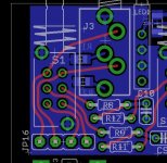
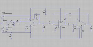
I had an idea on the new input select switch, the second image below. I've added PCB holes on both throws of the switch (JP16), including the one that is hardwired to the front panel 3.5mm jack. This allows for a whole bunch of fun optional combinations of parts:
* switch in: ODAC input (PCB hole pair 1); switch out: rear panel RCA input (PCB hole pair 2). Anything plugged into the 3.5mm would be in parallel with the rear RCA, so use one or the other.
* switch in: ODAC input (PCB hole pair 1); switch out: front panel 3.5mm via the hard wiring (nothing in PCB hole pair 2). Then ODAC out also run to the rear panel RCAs for ODAC line out in parallel with the amp input.
* No ODAC, batteries. switch in: rear panel RCA input (PCB hole pair 1); switch out: front panel 3.5mm jack via hardwiring.
etc....
Then regarding sgrossklass' good suggestion in post #14 to have some gain in the output stage, I've implementing it but in a special way. I want to keep the overall amp voltage gain in the low gain switch position unity (1x). So although I'm bumping the output stage votlage gain up to 1.33x, I'm actually decreasing the input stage gain to 0.75x = attenuation! This makes use of a poorly understood (at least it was by me a year ago) feature of inverting amps: unlike non-inverting stages they are stable below unity gain, all the way down to zero voltage gain in fact (full attenuation). Here is a great discussion about it on TI's engineering discussion forum:
https://e2e.ti.com/blogs_/archives/...verting-attenuator-g-0-1-uh-oh-is-it-unstable
The net result then is 0.75x voltage gain in stage 1 (a 7.5K feedback resistor with the 10K composite input resistor), times 1.33x gain in stage 2 (a 33K feedback resistor with the 24.9K input resistor) = 0.99x overall voltage gain (current buffer-only mode, same as with NwAvGuy's O2 in the low gain position).
Then in the "high" gain switch position the new feedback resistor is 18.7K in the input stage for a first stage voltage gain of 1.87x. Multiplied by the new second stage gain of 1.33 gives (still) 2.5x overall voltage gain, same as before and same as the most used high gain position in NwAvGuy's O2 headamp.
Then regarding sgrossklass' interesting suggestion to elminate the resistors to ground on the non-inverting inputs in post #18, I'm chickening out on this one and leaving the pads for the resistors. LTspice is having trouble converging with those inputs tied to ground directly that it doesn't with some resistance there. Probably just a simulation artifact, but there is also something rattling around in my head from way back when about trouble in tying some FET input op-amp inputs directly to ground. I can't remember why now, but I think it may have been voltage-to-substrate issues, in older FET inpu op amps. At any rate a jumper can simply be used in place of the resistor if anyone wants to tie those non-inverting inputs directly to ground. I am going to decrease resistors to 1K from 10K in the input stage and 5K from 24.9K in the output stage, which should at least help there with noise reduction.
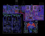
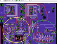
I've completely ripped up and re-done the layout around the headphone relay. In the old V3.0 layout in the first post in this thread a lot of the traces had to snake way to the left to get to the relay. Now the relay is centered, which shortens all those traces. The relay control circuitry is now on the left of the relay.
Plus I had a bit of a brainstorm on the relay circuit. In the ODA I have the relay coil looped through one pole of the on/off switch to peform the "no thump at turn off" function. It works wonderfully. There is no greater "advanced notice" of an amp power-down than the power switch, of course. Well here both poles of the switch are in use by the main circuit, preventing me from looping the relay coil through. Sure enough, although the turn-on thump is gone, there has been a small turn off thump. 3 pole right-angle PC-mount toggle switches exist, at least in the catalog, but not in stock at Mouser or Digikey. The 3 pole switch is also conisderably wider and wouldn't fit.
Well it hit me that one pole on the unused "thow" on the power switch in NwAvGuy's switch-in-the-middle design here can be used to shut down the relay control mosfet and nuke the output thump, similar to what I did with the ODA! The source on that relay control mosfet is already tied to the negative rail, which goes to one pole on the power switch. That switch is non-shorting, so tying the gate of that mosfet to the other "throw" on that pole causes the gate to be shorted to the source when the power switch is turned off. Mosfet goes off and so does the relay.
Then finally I've implemented another one of sgrossklass' suggestions in post #14, the clipping indicator (the stuff in the green circle, still a work in progress, but at this point at least I'm sure it will fit). I've used the clipping detect circuit from the ODA, which in turn came from various internet posts out there. I've made a compromise for space though. The ODA clipping circuit is "stereo", sensing both channels. Here I''m just going to make it "mono" on one channel, under the theory that if someone's source input is high enough to cause clipping it will probably be happening in both channels. Sensing the clipping on just one channel requires just a smaller a SOIC 8 chip instead of SOIC 14, plus saves two diodes.
Plus now the clipping circuit is going to be on the output stage, vs being on the input stage in the ODA. That works because of the first point above, the output stage now having gain, so it will be the first to clip as sgrossklass noted. Good stuff!
I've notched out the right rear corner of the PC board since the RCA jacks will have to be rear-panel mounted vertically to fit. No way to make them fit with either one PC board mounted. These are the REAN/Neutrik panel mount units with the 15.5mm insulating washers.
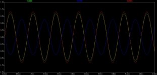
In the LTSpice plots green is the input source, blue is the output of the first stage, and red is the output of the second stage. In the transient plot I've used a 36K feedback resistor instead of 33K to bump the gain up slightly so the red trace would be visible vs. the input green trace. With 33K they would be on top of each other, of course. The peak of the input trace is 1.0V, the first stage output is 0.75V, and the output would be 1.0V again with 33K feedback. Note the output of the first (inverting) stage (blue trace) is 180 degrees out of phase vs. the (green) input, just like it is supposed to be, while the resultant (red) output trace is back in phase with the input after the second inversion.
In the AC plot the initial gain on the left axis is 0dB, while th initial phase on the right axis is zero degrees.
Here are bunch of modifications and additions on this project.
I had an idea on the new input select switch, the second image below. I've added PCB holes on both throws of the switch (JP16), including the one that is hardwired to the front panel 3.5mm jack. This allows for a whole bunch of fun optional combinations of parts:
* switch in: ODAC input (PCB hole pair 1); switch out: rear panel RCA input (PCB hole pair 2). Anything plugged into the 3.5mm would be in parallel with the rear RCA, so use one or the other.
* switch in: ODAC input (PCB hole pair 1); switch out: front panel 3.5mm via the hard wiring (nothing in PCB hole pair 2). Then ODAC out also run to the rear panel RCAs for ODAC line out in parallel with the amp input.
* No ODAC, batteries. switch in: rear panel RCA input (PCB hole pair 1); switch out: front panel 3.5mm jack via hardwiring.
etc....
Then regarding sgrossklass' good suggestion in post #14 to have some gain in the output stage, I've implementing it but in a special way.
I want to keep the overall amp voltage gain in the low gain switch position unity (1x). So although I'm bumping the output stage votlage gain up to 1.33x, I'm actually decreasing the input stage gain to 0.75x = attenuation! This makes use of a poorly understood (at least it was by me a year ago) feature of inverting amps: unlike non-inverting stages they are stable below unity gain, all the way down to zero voltage gain in fact (full attenuation). Here is a great discussion about it on TI's engineering discussion forum:https://e2e.ti.com/blogs_/archives/...verting-attenuator-g-0-1-uh-oh-is-it-unstable
The net result then is 0.75x voltage gain in stage 1 (a 7.5K feedback resistor with the 10K composite input resistor), times 1.33x gain in stage 2 (a 33K feedback resistor with the 24.9K input resistor) = 0.99x overall voltage gain (current buffer-only mode, same as with NwAvGuy's O2 in the low gain position).
Then in the "high" gain switch position the new feedback resistor is 18.7K in the input stage for a first stage voltage gain of 1.87x. Multiplied by the new second stage gain of 1.33 gives (still) 2.5x overall voltage gain, same as before and same as the most used high gain position in NwAvGuy's O2 headamp.
Then regarding sgrossklass' interesting suggestion to elminate the resistors to ground on the non-inverting inputs in post #18, I'm chickening out on this one and leaving the pads for the resistors.
LTspice is having trouble converging with those inputs tied to ground directly that it doesn't with some resistance there. Probably just a simulation artifact, but there is also something rattling around in my head from way back when about trouble in tying some FET input op-amp inputs directly to ground. I can't remember why now, but I think it may have been voltage-to-substrate issues, in older FET inpu op amps. At any rate a jumper can simply be used in place of the resistor if anyone wants to tie those non-inverting inputs directly to ground. I am going to decrease resistors to 1K from 10K in the input stage and 5K from 24.9K in the output stage, which should at least help there with noise reduction.I've completely ripped up and re-done the layout around the headphone relay. In the old V3.0 layout in the first post in this thread a lot of the traces had to snake way to the left to get to the relay. Now the relay is centered, which shortens all those traces. The relay control circuitry is now on the left of the relay.
Plus I had a bit of a brainstorm on the relay circuit.
In the ODA I have the relay coil looped through one pole of the on/off switch to peform the "no thump at turn off" function. It works wonderfully. There is no greater "advanced notice" of an amp power-down than the power switch, of course. Well here both poles of the switch are in use by the main circuit, preventing me from looping the relay coil through. Sure enough, although the turn-on thump is gone, there has been a small turn off thump. 3 pole right-angle PC-mount toggle switches exist, at least in the catalog, but not in stock at Mouser or Digikey. The 3 pole switch is also conisderably wider and wouldn't fit.Well it hit me that one pole on the unused "thow" on the power switch in NwAvGuy's switch-in-the-middle design here can be used to shut down the relay control mosfet and nuke the output thump, similar to what I did with the ODA!
The source on that relay control mosfet is already tied to the negative rail, which goes to one pole on the power switch. That switch is non-shorting, so tying the gate of that mosfet to the other "throw" on that pole causes the gate to be shorted to the source when the power switch is turned off. Mosfet goes off and so does the relay. Then finally I've implemented another one of sgrossklass' suggestions in post #14, the clipping indicator (the stuff in the green circle, still a work in progress, but at this point at least I'm sure it will fit). I've used the clipping detect circuit from the ODA, which in turn came from various internet posts out there. I've made a compromise for space though. The ODA clipping circuit is "stereo", sensing both channels. Here I''m just going to make it "mono" on one channel, under the theory that if someone's source input is high enough to cause clipping it will probably be happening in both channels. Sensing the clipping on just one channel requires just a smaller a SOIC 8 chip instead of SOIC 14, plus saves two diodes.
Plus now the clipping circuit is going to be on the output stage, vs being on the input stage in the ODA. That works because of the first point above, the output stage now having gain, so it will be the first to clip as sgrossklass noted. Good stuff!
I've notched out the right rear corner of the PC board since the RCA jacks will have to be rear-panel mounted vertically to fit. No way to make them fit with either one PC board mounted. These are the REAN/Neutrik panel mount units with the 15.5mm insulating washers.
In the LTSpice plots green is the input source, blue is the output of the first stage, and red is the output of the second stage. In the transient plot I've used a 36K feedback resistor instead of 33K to bump the gain up slightly so the red trace would be visible vs. the input green trace. With 33K they would be on top of each other, of course. The peak of the input trace is 1.0V, the first stage output is 0.75V, and the output would be 1.0V again with 33K feedback. Note the output of the first (inverting) stage (blue trace) is 180 degrees out of phase vs. the (green) input, just like it is supposed to be, while the resultant (red) output trace is back in phase with the input after the second inversion.
In the AC plot the initial gain on the left axis is 0dB, while th initial phase on the right axis is zero degrees.
Attachments
Last edited:
- Status
- This old topic is closed. If you want to reopen this topic, contact a moderator using the "Report Post" button.
- Home
- Amplifiers
- Headphone Systems
- An inverting version of the NwAvGuy O2 headphone amp vs. the original: THD+N