Err, wait a microsecond.Plus now the clipping circuit is going to be on the output stage, vs being on the input stage in the ODA. That works because of the first point above, the output stage now having gain, so it will be the first to clip as sgrossklass noted. Good stuff!")
That's only true if you leave the volume turned up all the way (which often is not the case in practice). Still, at a maximum input gain of 1.87x, odds are that even a rev. B ODAC on high gain during battery operation won't clip the input stage.
I'm not such a fan of output noise levels with the inverting output stage at 1.33x gain. Those compute to about 6 µVrms, about 10 dB higher than the stock O2. Not bad at all, but you're probably going to notice slight hiss on very sensitive IEMs (think 130-ish dB/V). You could shave off a few dB again by investing into a low-noise buffer stage (maybe using a '2068) right after the pot, no more than about 5-6 dB though. That one obviously takes extra power, too.
I think if you want extra gain in the output stage, you really are best off with non-inverting operation, a low(ish)-noise OP and a bit more than 1.33x. And preferably a (diamond) buffer inside the loop, though that obviously no longer is jellybean territory if you don't want current consumption to explode.
The twice-inverting input stage may not be such a bad idea after all - you could get away with relatively low-power opamps in there. For one of them, at least. Maybe a bit of gain with a TLE2072 and 10k/22k at first, and then another at 22k/22k or so. Or TLE2062 + TLE2072 even (could be a bit noisy though), or TLE2072 + TLE2064 (for 2 channels in parallel at a measly 1.25 mA per quad), or TLE2072 + NJM2068 / MC33078 (TI) or LM833P (TI) / whatever. So many permutations to try out. Hmm. Are there any more cheap, halfway modern, decent low-power bipolars (similar to the TLEs but with a different frontend)? MC33178 has this fat, underbiased output stage, so that's not an option. 4560s are getting a bit old. OPA16xx are all surface mount.
Random thought on volume pots: I'm under the impression that hi-fi manufacturers like to use 50k or even 100k over 20k or 10k due to better channel matching at low volumes. Why this should be so, I'm not sure - wouldn't lower-impedance parts have thicker and hence theoretically better-controlled tracks?
Thanks again for the suggestions! Much appreciated.
I've actually gone to linear pots these days to get better tracking. I'm using a dual linear 1K in the ODA amp mainly for power handling (50mW vs. 25mW for audio taper) and 1K audio tapers are non-stocking at the distributors, but as a side benefit the tracking is 10% vs. 20% with the audio taper, as I recall. From what I read using linear taper pots are a somewhat-common thing in guitar amps. In this amp I'm going to have a 5K dual linear-taper 9mm as the "standard" part, with a 5K dual audio-taper 9mm listed as an alternate.
Good points about the relative levels after the input and output stages with some typical input sources! After I did that post it hit me that I should have included some typical numbers. With with the 2Vrms maximum that is supposeed to come out of a CD we have 2Vrms * 1.87 = 3.74Vrms = 5.3Vpeak from the first stage in high-gain mode. With fully charged batteries that is OK at +/-8.4Vdc nominal to 10.1Vdc fully charged. Keep in mind the AC rails in this amp are +/-15Vdc vs. the +/-12Vdc in the O2 amp, so no troubles at all on AC. But... with nearly discharged batteries at +/-7Vdc the 5.3Vpeak might be a problem given 2V or so of output stage overhead in the LME49880 chip, espeically with the 5K load (the pot) on each channel. However a 5.3Vpeak would mean 5.3Vpeak * 1.33 = 7V peak at the output stage. It would have clipped several volts before the input stage and turned on the clipping indicator.
Good thoughts about the lower noise with a non-inverting output stage. I fully agree it would be lower noise, but I want to keep this one with all inverting stages. Even though it will mean a higher noise floor. In all the posts I've seen here on the forum here over the past few years using LME49600 or BUF634 current buffers, I can't recall a single one using an inverting "op-amp plus buffer" topology. This one is more of a test-bed for inverting stages.
NwAvGuy was shooting for lowest noise floor. I think he pretty well achieved that with the O2 and the non-inverting stages. Best I can recall the one PM I did with him on "have you considered inverting stages" I think noise floor is what he cited as why he went with non-inverting, but I'm pretty sure he wrote something to the effect of still considering inverting for the future.
However, lemme think about it. Maybe I can find a layout way to wire up the output stage as either inverting or non-inverting with a couple of jumpers. It would be kind of fun to be able to run the output stage as either!
I've actually gone to linear pots these days to get better tracking. I'm using a dual linear 1K in the ODA amp mainly for power handling (50mW vs. 25mW for audio taper) and 1K audio tapers are non-stocking at the distributors, but as a side benefit the tracking is 10% vs. 20% with the audio taper, as I recall. From what I read using linear taper pots are a somewhat-common thing in guitar amps. In this amp I'm going to have a 5K dual linear-taper 9mm as the "standard" part, with a 5K dual audio-taper 9mm listed as an alternate.
Good points about the relative levels after the input and output stages with some typical input sources! After I did that post it hit me that I should have included some typical numbers. With with the 2Vrms maximum that is supposeed to come out of a CD we have 2Vrms * 1.87 = 3.74Vrms = 5.3Vpeak from the first stage in high-gain mode. With fully charged batteries that is OK at +/-8.4Vdc nominal to 10.1Vdc fully charged. Keep in mind the AC rails in this amp are +/-15Vdc vs. the +/-12Vdc in the O2 amp, so no troubles at all on AC. But... with nearly discharged batteries at +/-7Vdc the 5.3Vpeak might be a problem given 2V or so of output stage overhead in the LME49880 chip, espeically with the 5K load (the pot) on each channel. However a 5.3Vpeak would mean 5.3Vpeak * 1.33 = 7V peak at the output stage. It would have clipped several volts before the input stage and turned on the clipping indicator.
Good thoughts about the lower noise with a non-inverting output stage. I fully agree it would be lower noise, but I want to keep this one with all inverting stages. Even though it will mean a higher noise floor. In all the posts I've seen here on the forum here over the past few years using LME49600 or BUF634 current buffers, I can't recall a single one using an inverting "op-amp plus buffer" topology. This one is more of a test-bed for inverting stages.
NwAvGuy was shooting for lowest noise floor. I think he pretty well achieved that with the O2 and the non-inverting stages. Best I can recall the one PM I did with him on "have you considered inverting stages" I think noise floor is what he cited as why he went with non-inverting, but I'm pretty sure he wrote something to the effect of still considering inverting for the future.
However, lemme think about it.
Maybe I can find a layout way to wire up the output stage as either inverting or non-inverting with a couple of jumpers. It would be kind of fun to be able to run the output stage as either!
Last edited:
Output stage now inverting or (optionally) non-inverting
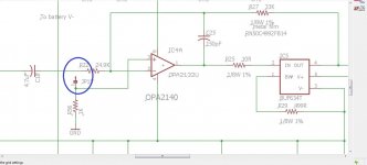
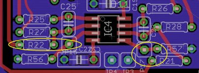
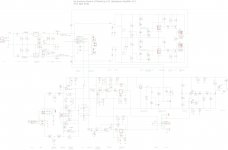
I've followed up on the suggestion sgrossklass made of having a non-inverting ouput stage. Turns out adding a single PC hole on each channel for a jumper allows the stage to be optionally wired as either inverting or non-inverting. With a non-inverting output buffer stage the final signal output would be inverted, of course, since the gain stage still inverts. With the inverting output stage the final signal is non-inverting.
The non-inverting configuaration here will just be a 1x voltage gain current buffer, no voltage gain as with the inverting configuration.
In the circuit snippet below, to change from inverting to non-inverting:
* Remove R22
* Jumper the new point JP15 (the blue circle) to the pad on the end of R22 closest to the coupling capacitor.
* Replace R56 with a 24.9K resistor. This becomes the input bias current ground return resistor for the non-inverting op-amp input. The pot is 5K, so a 24.9K resistor here.
* Replace the feedback resistor R27 with a 1K.
* The other channel is similar.
Attachments
Last edited:
This thing sounds amazing!
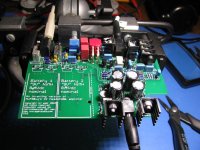
I just finished building up V3.5 after the board arrived from fab yesterday and it sounds great. I've implemented it as discussed above, with the first inverting stage attenuating (0.75X) in the low gain position, then the output inverting stage with 1.32x gain for an overall gain of unity. The high gain position is (18.7K/(4.99K + 4.99K)) = 1.87x, for a total of 1.87 * 1.32 = 2.5x. So the net result is the same two most popular gain positions from NwAvGuy's O2, 1x and 2.5x.
Makes me sad this LME49880 FET input chip is going away, thanks to the TI "chippocalypse". First I've messed with it. I have to say I'm mighty impressed.
I'm not going to post the Gerbers quite yet. It does fit in the B5-080 case just fine, but I'm thinking about eliminating the batteries entirely, just using that area only for the ODAC (which also fits just fine). That change would also eliminate all the power management SMD parts under the batteries leaving only the 3 op-amps and a few bypass caps as SMD. 95% of it is through-hole without the PM stuff.
I just finished building up V3.5 after the board arrived from fab yesterday and it sounds great.
I've implemented it as discussed above, with the first inverting stage attenuating (0.75X) in the low gain position, then the output inverting stage with 1.32x gain for an overall gain of unity. The high gain position is (18.7K/(4.99K + 4.99K)) = 1.87x, for a total of 1.87 * 1.32 = 2.5x. So the net result is the same two most popular gain positions from NwAvGuy's O2, 1x and 2.5x.Makes me sad this LME49880 FET input chip is going away, thanks to the TI "chippocalypse".
First I've messed with it. I have to say I'm mighty impressed.I'm not going to post the Gerbers quite yet. It does fit in the B5-080 case just fine, but I'm thinking about eliminating the batteries entirely, just using that area only for the ODAC (which also fits just fine). That change would also eliminate all the power management SMD parts under the batteries leaving only the 3 op-amps and a few bypass caps as SMD. 95% of it is through-hole without the PM stuff.
Attachments
-
 IMG_3736.JPG563.6 KB · Views: 401
 -
 IMG_3737.JPG514.4 KB · Views: 386
 -
 IMG_3738.JPG426.3 KB · Views: 385
 -
 IMG_3739.JPG409.1 KB · Views: 142
 -
schematic.pdf72.1 KB · Views: 89
-
 schematic.jpg533.1 KB · Views: 188
 -
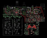
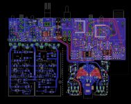 layout.jpg1,009.6 KB · Views: 159
 -
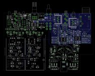
 layer 1 top.jpg1,002.7 KB · Views: 139
 -
 layer 2 V+.jpg1,007.1 KB · Views: 95
 -
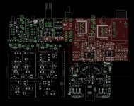 layer 3 V-.jpg1,002.3 KB · Views: 107
Last edited:
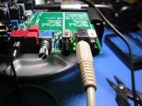
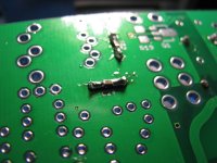
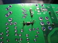
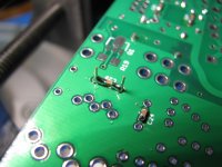
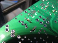
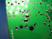
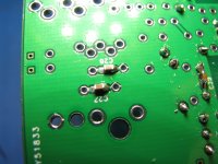
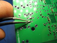
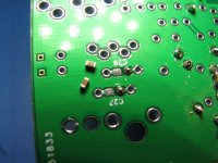
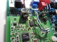
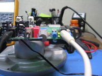
Soldering in the 0603 bypass caps under the board
Here are some pictures I've been meaning to post from the last build. I now have 0603-sized SMD 1uF MLCC bypass caps underneath the board, between the through-hole leads of each 0.22uF film cap. There is one of these 2-capacitor combos on each power rail on each chip.
I've had a chance now to spend some time with the scope studying the output of both the gain stage and output stage. I've loaded the output with various headphones, cable lengths, and capacitors up to 2200pF (and zero series output resistance on the BUF634's). No oscillations at all, at least up the 200mHz bandwidth of the scope, so apparently something is working here with the bypassing - and loop stability of the OPA2140 + BUF634's.
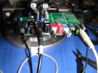
The SMD caps should be soldered in first, as the photos show.
* 3728 shows two of the 0603 pads under the board for C27 and C28, along with the caps. I've put a small solder blob on one end of each part's pad. Some care is needed here to avoid splashing solder on the through-holes for the film cap and plugging them up. If that happens the fix is easy. Just heat that hole while you stick in the lead of the film cap. Walk it down the hole, if necessary, by re-heating the through hole as needed.
* 3729 & 3730 show heating up those two blobs and sticking in one end of each part, holding the capacitor with the tweezers.
* In 3731 I've soldered the other end of the two capacitors.
* 3732 shows soldering the film capacitor's through-hole leads. Here I actually did plug one through-hole with solder while soldering the SMD cap, as the photo shows. I used the technique above of heating the through-hole and walking the lead down to get that through-hole lead in.
* In 3733 I've solder-flooded the gap between the through-hole leads and the SMD capacitor on purpose, just because I could. It isn't necessary to do this. In 3734 I have a photo of two leads just soldered by themselves. 3735 shows the same two leads subsequently flooded (on purpose). I'm doing that just to help reduce trace inductance. Normally having a bypass cap on the other side of a through-hole isn't the best in terms of through-hole inductance, but here the film cap's through-hole lead goes through which should help. Threre wouldn't be space available on the top of this board for the SMD cermics along with the film caps. Doing things this way gets around the space limitations. At any rate the results are what matters.
Here are some pictures I've been meaning to post from the last build. I now have 0603-sized SMD 1uF MLCC bypass caps underneath the board, between the through-hole leads of each 0.22uF film cap. There is one of these 2-capacitor combos on each power rail on each chip.
I've had a chance now to spend some time with the scope studying the output of both the gain stage and output stage. I've loaded the output with various headphones, cable lengths, and capacitors up to 2200pF (and zero series output resistance on the BUF634's). No oscillations at all, at least up the 200mHz bandwidth of the scope, so apparently something is working here with the bypassing - and loop stability of the OPA2140 + BUF634's.
The SMD caps should be soldered in first, as the photos show.
* 3728 shows two of the 0603 pads under the board for C27 and C28, along with the caps. I've put a small solder blob on one end of each part's pad. Some care is needed here to avoid splashing solder on the through-holes for the film cap and plugging them up. If that happens the fix is easy. Just heat that hole while you stick in the lead of the film cap. Walk it down the hole, if necessary, by re-heating the through hole as needed.
* 3729 & 3730 show heating up those two blobs and sticking in one end of each part, holding the capacitor with the tweezers.
* In 3731 I've soldered the other end of the two capacitors.
* 3732 shows soldering the film capacitor's through-hole leads. Here I actually did plug one through-hole with solder while soldering the SMD cap, as the photo shows. I used the technique above of heating the through-hole and walking the lead down to get that through-hole lead in.
* In 3733 I've solder-flooded the gap between the through-hole leads and the SMD capacitor on purpose, just because I could.
It isn't necessary to do this. In 3734 I have a photo of two leads just soldered by themselves. 3735 shows the same two leads subsequently flooded (on purpose). I'm doing that just to help reduce trace inductance. Normally having a bypass cap on the other side of a through-hole isn't the best in terms of through-hole inductance, but here the film cap's through-hole lead goes through which should help. Threre wouldn't be space available on the top of this board for the SMD cermics along with the film caps. Doing things this way gets around the space limitations. At any rate the results are what matters.Attachments
Last edited:
Hello!
I have asked if I could listen to the new inverting O2 amp and I was graciously sent AGDR's amp and have had it for a few days now. I cant thank AGDR enough for sending it to me for a comparison to my O2's, ODA, Bottlehead Crack with Speedball and a few other amps I have.
I built an O2 a few years back and use it with a rev a ODAC, I also have a "built" O2 as well, one is AC only the other is AC and batteries. The ODA was built on AGDR's fab board and I have enjoyed it for many months now.
Coming from a ancient tube background, I was always curious to hear how a good tube amp would sound compared to these solid state amps...I went thru many headphones and after a few years if buying and selling I have settled on a pair of Beyerdynamics T90's 250 ohms...
This lead to reading many posts on how well these T90's pair with the Bottlehead Crack amp....so after awhile my curiosity forced me to buy a Crack kit..I enjoyed building the ODA and working with AGDR and many DIY'ers in getting it up and running. Its a stellar amp for sure.
So after building the Crack and adding the cascode constant current source mod called "Speedball" I was impressed at how good it sounded with the high impedance T90's...The crack design is an OTL one....not good for low impedance cans....it sounds like a marraige made in heaven..I have gone thru many tubes and lots of listening and its definitely a great pairing.
So let me leave it hear for now and I will post later today my experiences with the inverting O2....
All the best
Alex
Normally before I do any comparisons I try to set things up so we are comparing apples to apples...same sound volume levels, same cables, same source material etc....but this time I just wanted to hear the new version....so....
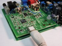
I plugged it to one of my several pc's running Win10 and the amp has a Rev B ODAC wired up already so it was easy to just attach a USB cable, start up my music player JRiver and select some familiar demo material.
It doesnt take long for me to make a preliminary judgement of how something sounds...subjectively that is.
I know AGDR has measured this amp and made comparisons to the original O2 and the original O2 has better specs...but this time I wanted to know how it sounded, specs be dammed! LOL.
The Crack Tube amp with its higher THD and inherent tube noise attributes still sounds very musical and with high impedance cans just does wonderfully. A sonic dream.
So would the new inverting O2 provide the same type of listening experience...
Well right off the bat I was really amazed at the sound I was hearing....absolutely stellar.
Like AGDR stated in a few posts earlier..."This thing sounds amazing!" It does. After 30 minutes of going thru several well recorded and mastered cuts I made a decision that somehow I had to have or build one of these!!!
I spent an hour listening to 30 or so songs....using material I have from several really anal audio jocks that go way beyond what I do with high end stuff...but the material I have from them is really really good stuff...lots of demo's from major audio speaker makers, cable vendors etc....
The amp is totally clean and silent, pause the music, crank up the volume and gain to hige setting, there is no audible hiss or hum...this amp is AC only with 15 volt rails...this is with both 250 ohm and 38 Ohm headphones.
The subjective words come to mind: Transparent, Open, Clear, Sparkle, Crisp, 3 Dimensional etc...more than enough power to cause pain in listening....I was wondering how so few parts could sound so good...
Usually something new seems to always sound good...its after a few days and going to a more controlled setting and comparing to other amps does the reality set it that the item may be great but so are many other items ( in this case amps).
So I then turned on the Crack, the ODA and my O2's ...and proceed to swap things in and out to see how the inverting O2 compared to the other amps. Mind you this is all subjective and my opinion....this coming from a real objective person !! LOL...
I have a good supply of well recorded and mastered source material that I have collected over the years from varios audiophiles, audio speaker OEM's and audio equipment vendors...used to demo their stuff...I started with a commercial CD by Al DiMeola, his Kiss My Axe album, the first two cuts, South Bound Traveler and The Embrace are just wonderful to use for comparisons. Great openess, transparent, shimmering sounds, tight precussion and huge bass notes....
The inverting O2 is a magical amp, it sounds more open and accurate but musical all at the same time....better than the Crack which I hear less clarity, harder to hear the details, it seems like its sound is more constrictive and is trying hard to get it all out, where the inverting O2 is just effortless and flowing...the clarity and openess allows for a more real experience...makes you want to listen to all of your music again to see what you may have been missing!
No I am not selling my Crack.....but I would choose the inverting O2 to listen to first for sure.
I then compared the original O2, which sound very similar to the inverting version, but its just not as good sounding...just a little less dynamic range at the same volume settings...just a little harder to grasp the details and the soundstage is just not as good and the inverting version. The ODA seesms to be very much like the original O2...I compared the ODA awhile back in a blind AB test, I could not tell the difference bewteen the two....The original O2 is still a very good amp.
But this to me is the joy of being able to have several amps, dacs etc..to be able to build and compare things and enjoy them all. Being an objective persion and wanting the best specs sometimes just gets too boring!! LOL!
In conclusion, I will put one of these inverting O2's together someday and it will have a special place in my headamp collection! I think AGDR has hit upon a wonderful twist on the O2, using this inverting design has indeed worked out well....and no I dont need the batteries!! Ha!! (note...have to get the power switch reversed...lol)....
All the best
Alex
Last edited:
Mounting an ODAC on the board
Alex - thank you very much for posting the review! I know it takes a lot of time and effort to do listening comparisons.
When I sent the board to Alex I said this in the email:
"So give it a listen and let me know what you think!! Please be perfectly frank! If it s*cks, please do tell me it s*cks! I’m especially curious what you think vs. the crack amp, since this one has FET chips. Who knows, the crack may very well come out ahead!"
So I'm happy - and relieved, lol! - that it compared favorably.
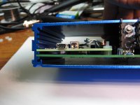
Below are some photos of installing the ODAC board. Goes on the same way as the O2. Even if I leave batteries out of the final version I will still likely include two battery terminals to backstop the board mechanically, just like NwAvGuy did in the O2 headamp.
* 35, 36, and 37 show the ODAC mounted on the board. In the next board revision I have the ground holes for the ODAC-to-O2 wire bundle right under the PCB holes for the signal lines. In this revision the ground holes were half and inch away. The ODAC wires up same was with the O2, with one signal and one ground line twisted together and routed to the Inverting O2 PC board.
The ODAC board (this one is George's rev B board) mounts the same was as with the O2, with one bolt through the hole and the left side in a case slot, plus the battery terminals backstopping it. I've used #4 nylon hardware here, but the holes (both in the ODAC and the inverting PC board) are actually M3 metric. Just turned out all my M3 nylon bolts were only 6mm long. Needs to be around 8mm. These are 3/8 long bolts as I recall.
* 38 shows the ODAC board in the case slot. I've used two nylon #4 washers as spacers. One nylon nut was not tall enough, but two were too tall. The two washers make the board closer to level. To get the ODAC board completely level it will be necessary to sand or file the face of one nylon washer a bit. Just a reminder that those two heat sinks on the rear voltage regulators sticking out the back of the case are temporary, just placeholders for the rear panel.
* 49 doesn't have a thing to do with headphones. I just got a laugh out of this one while doing some PCB soldering and snapped it.
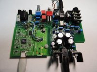
The wires sticking out the front on the board in #35 solved a problem that I found in testing. The turn-on anti-thump worked great, but I was still getting a turn off thump. I eventually realized the reason was that I had no electrolytic capactors on the power supply rails after the power switch. There was nothing to keep the rails up long enough to allow the headphone relay to close, lol. Adding two small electrolytics to the rails via those wires solved it. On the next board revision the electros will be on the board.
I'm now using a vertical 3.5mm jack on the output with an insulated nose as can be seen in #35. No need any longer for an exceptionally large front panel hole around that nose to keep it from touching, as I did with the ODA amp. I have the input section and output section on different ground star segments. I didn't want to the two also connecting via the front panel. The input 3.5mm jack is the same metal threaded nose as the ODA. It grounds the front panel (and case) to the input section via the jack's nut same as the ODA.
Alex - thank you very much for posting the review!
I know it takes a lot of time and effort to do listening comparisons. When I sent the board to Alex I said this in the email:
"So give it a listen and let me know what you think!! Please be perfectly frank! If it s*cks, please do tell me it s*cks! I’m especially curious what you think vs. the crack amp, since this one has FET chips. Who knows, the crack may very well come out ahead!"
So I'm happy - and relieved, lol! - that it compared favorably.
Below are some photos of installing the ODAC board. Goes on the same way as the O2. Even if I leave batteries out of the final version I will still likely include two battery terminals to backstop the board mechanically, just like NwAvGuy did in the O2 headamp.
* 35, 36, and 37 show the ODAC mounted on the board. In the next board revision I have the ground holes for the ODAC-to-O2 wire bundle right under the PCB holes for the signal lines. In this revision the ground holes were half and inch away. The ODAC wires up same was with the O2, with one signal and one ground line twisted together and routed to the Inverting O2 PC board.
The ODAC board (this one is George's rev B board) mounts the same was as with the O2, with one bolt through the hole and the left side in a case slot, plus the battery terminals backstopping it. I've used #4 nylon hardware here, but the holes (both in the ODAC and the inverting PC board) are actually M3 metric. Just turned out all my M3 nylon bolts were only 6mm long. Needs to be around 8mm. These are 3/8 long bolts as I recall.
* 38 shows the ODAC board in the case slot. I've used two nylon #4 washers as spacers. One nylon nut was not tall enough, but two were too tall. The two washers make the board closer to level. To get the ODAC board completely level it will be necessary to sand or file the face of one nylon washer a bit. Just a reminder that those two heat sinks on the rear voltage regulators sticking out the back of the case are temporary, just placeholders for the rear panel.
* 49 doesn't have a thing to do with headphones. I just got a laugh out of this one while doing some PCB soldering and snapped it.
The wires sticking out the front on the board in #35 solved a problem that I found in testing. The turn-on anti-thump worked great, but I was still getting a turn off thump. I eventually realized the reason was that I had no electrolytic capactors on the power supply rails after the power switch. There was nothing to keep the rails up long enough to allow the headphone relay to close, lol. Adding two small electrolytics to the rails via those wires solved it. On the next board revision the electros will be on the board.
I'm now using a vertical 3.5mm jack on the output with an insulated nose as can be seen in #35. No need any longer for an exceptionally large front panel hole around that nose to keep it from touching, as I did with the ODA amp. I have the input section and output section on different ground star segments. I didn't want to the two also connecting via the front panel. The input 3.5mm jack is the same metal threaded nose as the ODA. It grounds the front panel (and case) to the input section via the jack's nut same as the ODA.
Attachments
Last edited:
Maybe we need a contest to come up with a CAT acronym? LOL!
Well since it has two inverting stages maybe the "double black cat version" lol.
The one on the left with the longer tail is a copy cat. She spends all day following her sister around and doing whatever her sister does.
Attachments


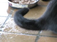
Well since it has two inverting stages maybe the "double black cat version" lol.
The one on the left with the longer tail is a copy cat. She spends all day following her sister around and doing whatever her sister does.
O2CAT
But it sounds like AutoCAD
O2CAT
Lol!
The analogy is better than I realized. Copy cat is big and beefy, but only unity gain.
So there is the output stage. Her little sister who is the brains of the operation is the input/gain stage.Update, V3.6 board, clipping circuit change
Here is an update on this project. I know a couple of folks are interested.
The new V3.6 boards were done on Tuesday. Once the good folks in China finally deliver them to FedEx I should be able to build and test a V3.6 next week with any luck.
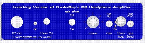
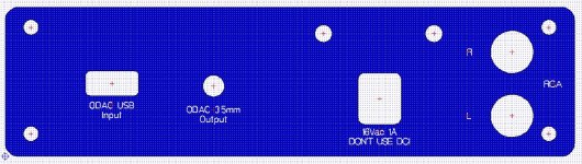
I have a first pass at the panels done and into Front Panel Express, image below. I have a high degree of confidence in the front panel, but somewhat less in the rear. Turns out there is, in fact, enough room for the nice Rean insulated RCA jacks but just *barely* in all dimensions. Should just exactly fit, according to the mechanicals, but we will see how real life turns out.
I have a set of materials out at a new Google Drive folder now too, here:
https://drive.google.com/folderview?id=0B67cJELZW-i8S1VmUzZsUGZZN00&usp=sharing
(V3.6 folder) but I would caution everyone not to make any purchases based on those yet - things could still change. But at least it gives a look. I'm still adding to the build instructions, although what is there has been checked and should be accurate.
I discovered a conceptual hiccup in the clipping circuit before sending V3.6 out and corrected it. If a two stage amp like this or NwAvGuy's O2 has a unity gain output stage, then monitoring clipping on the input gain stage is enough. That is the way I have things set up in my ODAC amp.
BUT... if the second stage has gain that goes out the window it turns out. Having gain on the output stage is a more general case. Consider the situation where we have the +/-15.3Vdc rails here. Lets say both the gain stage and output stage go up to 13.5V before clipping.
So assume you have an input signal plus voltage gain such that the peak output of the gain stage is 13.0Vdc, 0.5Vdc before clipping. Great. But if the output stage has the 1.33x voltage gain then the output stage will be at 13.0 * 1.33 = 17.3Vdc and clipping. A clipping detect circuit that is only on the input stage wouldn't do the job.
Conversely assume the input stage is trying to hit 14.0 volts on peaks and is clipping at the 13.5Vdc maximum. But if the volume control (which is in the middle of the amp of course, like the O2) is turned down 1/3 of the way the output stage would be at (13.5 * 0.33) * 1.33 = 12.03Vdc. A clipping detector set at 13.50Vdc would miss it, even with the signal going into the output stage clipped. So the clipping detector can't be only on the output stage either, as I originally had it.
The solution is going back to the clipping circuit I have in the ODAC which used the quad 14 pin chip and effectively logically ORs the two sections together. In the ODAC those are gain stage right and left channel. Here one input is from a channel on the gain stage, while the other is the same channel on the output stage. So if either the gain stage OR output stage clip it will now be detected.
Another change in V3.6 is an additional set of pass-through wiring holes behind the input select switch. The holes make it easy to wire the ODAC output to both the amp input and the rear panel RCA jacks. Yet another change is that I've gone through the whole thing and managed to "flatten" several of the vertical/tombstoned parts. The batteries are gone now, which has provided some more space to improve the layout in a couple of places.
Here is an update on this project. I know a couple of folks are interested.
The new V3.6 boards were done on Tuesday. Once the good folks in China finally deliver them to FedEx I should be able to build and test a V3.6 next week with any luck.
I have a first pass at the panels done and into Front Panel Express, image below. I have a high degree of confidence in the front panel, but somewhat less in the rear. Turns out there is, in fact, enough room for the nice Rean insulated RCA jacks but just *barely* in all dimensions. Should just exactly fit, according to the mechanicals, but we will see how real life turns out.
I have a set of materials out at a new Google Drive folder now too, here:
https://drive.google.com/folderview?id=0B67cJELZW-i8S1VmUzZsUGZZN00&usp=sharing
(V3.6 folder) but I would caution everyone not to make any purchases based on those yet - things could still change. But at least it gives a look. I'm still adding to the build instructions, although what is there has been checked and should be accurate.
I discovered a conceptual hiccup in the clipping circuit before sending V3.6 out and corrected it.
If a two stage amp like this or NwAvGuy's O2 has a unity gain output stage, then monitoring clipping on the input gain stage is enough. That is the way I have things set up in my ODAC amp.BUT... if the second stage has gain that goes out the window it turns out. Having gain on the output stage is a more general case. Consider the situation where we have the +/-15.3Vdc rails here. Lets say both the gain stage and output stage go up to 13.5V before clipping.
So assume you have an input signal plus voltage gain such that the peak output of the gain stage is 13.0Vdc, 0.5Vdc before clipping. Great. But if the output stage has the 1.33x voltage gain then the output stage will be at 13.0 * 1.33 = 17.3Vdc and clipping. A clipping detect circuit that is only on the input stage wouldn't do the job.
Conversely assume the input stage is trying to hit 14.0 volts on peaks and is clipping at the 13.5Vdc maximum. But if the volume control (which is in the middle of the amp of course, like the O2) is turned down 1/3 of the way the output stage would be at (13.5 * 0.33) * 1.33 = 12.03Vdc. A clipping detector set at 13.50Vdc would miss it, even with the signal going into the output stage clipped. So the clipping detector can't be only on the output stage either, as I originally had it.
The solution is going back to the clipping circuit I have in the ODAC which used the quad 14 pin chip and effectively logically ORs the two sections together. In the ODAC those are gain stage right and left channel. Here one input is from a channel on the gain stage, while the other is the same channel on the output stage. So if either the gain stage OR output stage clip it will now be detected.
Another change in V3.6 is an additional set of pass-through wiring holes behind the input select switch. The holes make it easy to wire the ODAC output to both the amp input and the rear panel RCA jacks. Yet another change is that I've gone through the whole thing and managed to "flatten" several of the vertical/tombstoned parts. The batteries are gone now, which has provided some more space to improve the layout in a couple of places.
Attachments
Last edited:
I would agree, it does look a bit cluttered! The constraints of the box. The good news it is all still functional, even with the close spacing. All the front panels parts are the same spacings as the existing V3.5 and I've tried it out with various plug types inserted (different overmolds and metal shells). All seeems to fit OK. The 3.5mm input has to stay since I have a several 3.5mm sources around.
The one front-panel thing I would like to change if I can find a way someday is that stacked green LED power indicator. The top one wound up inside the countersink ring of the jack. That still works OK, the depth of the countersink leaves 1.2mm of metal and the LED only sticks out 0.8mm into the panel. The light should still be visible around the nut edge. On some future version (not anytime soon, lol, that would be a V4.0 someday) I could probably scoot all the board edge parts left a bit since there is a few mm of space between the 1/4" jack and the case edge.
Another thought I've recently had is move the 4.7uF coupling caps somewhere else, down along the spacing between the amp section and ODAC. The would free up several mm of panel space. Just getting the LED moved left would make the panel look a lot less cluttered.
The good news it is all still functional, even with the close spacing. All the front panels parts are the same spacings as the existing V3.5 and I've tried it out with various plug types inserted (different overmolds and metal shells). All seeems to fit OK. The 3.5mm input has to stay since I have a several 3.5mm sources around.The one front-panel thing I would like to change if I can find a way someday is that stacked green LED power indicator. The top one wound up inside the countersink ring of the jack. That still works OK, the depth of the countersink leaves 1.2mm of metal and the LED only sticks out 0.8mm into the panel. The light should still be visible around the nut edge. On some future version (not anytime soon, lol, that would be a V4.0 someday) I could probably scoot all the board edge parts left a bit since there is a few mm of space between the 1/4" jack and the case edge.
Another thought I've recently had is move the 4.7uF coupling caps somewhere else, down along the spacing between the amp section and ODAC. The would free up several mm of panel space. Just getting the LED moved left would make the panel look a lot less cluttered.
Last edited:
V3.6 works! I'll post the Gerbers
The V3.6 PC boards for this project arrived yesterday. I've built one up and...works perfectly! I'll go ahead and post the Gerbers at the project Google Drive link.
I've taken a large number of build photos that match up with each one of the build-up assembly steps in the build instructions. I'll post those also out in the "photos" folder at the Google Drive link. I've listed the steps by size of the parts. The first step is the few SMD parts, all on the back of the board. Then the "flat" through-hole parts like the 1/8W resistors. Then taller stuff like the 0.22uF film caps, then even taller parts like the push button switches, etc. By building it up this way the taller parts don't get in the way of the shorter parts.
The first pass at the front and rear panel won't arrive for a couple of weeks yet. If they work I'll post the FPE CAD files, but if not then there will be another pass involved.
It took three board turns, but I'm pretty happy with the results. Adding the two 330uF electrolytics after the power switch solved the turn-off thump problem. The rails stay up long enough now for the headphone relay to turn off. Zero turn-on and turn-off thumps now. I reduced the length of the slots for the power jack another 0.5mm and that worked out great. Very little play now in the slots before soldering.
I have 6 extra PC boards from this run that I'll sell at-cost plus actual shipping cost if anyone is interested. Just send me a PM. I had 10 boards done (4 layer, gold [ENIG] finished) at Seeed Studio for a total of $164 USD including the FedEx shipping, so $16 a board.
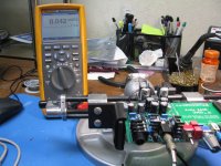
The last photo is the DC offset. 42 MICROvolts on each channel!
The V3.6 PC boards for this project arrived yesterday. I've built one up and...works perfectly!
I'll go ahead and post the Gerbers at the project Google Drive link. I've taken a large number of build photos that match up with each one of the build-up assembly steps in the build instructions. I'll post those also out in the "photos" folder at the Google Drive link. I've listed the steps by size of the parts. The first step is the few SMD parts, all on the back of the board. Then the "flat" through-hole parts like the 1/8W resistors. Then taller stuff like the 0.22uF film caps, then even taller parts like the push button switches, etc. By building it up this way the taller parts don't get in the way of the shorter parts.
The first pass at the front and rear panel won't arrive for a couple of weeks yet. If they work I'll post the FPE CAD files, but if not then there will be another pass involved.
It took three board turns, but I'm pretty happy with the results. Adding the two 330uF electrolytics after the power switch solved the turn-off thump problem. The rails stay up long enough now for the headphone relay to turn off. Zero turn-on and turn-off thumps now. I reduced the length of the slots for the power jack another 0.5mm and that worked out great. Very little play now in the slots before soldering.
I have 6 extra PC boards from this run that I'll sell at-cost plus actual shipping cost if anyone is interested. Just send me a PM.
I had 10 boards done (4 layer, gold [ENIG] finished) at Seeed Studio for a total of $164 USD including the FedEx shipping, so $16 a board. The last photo is the DC offset. 42 MICROvolts on each channel!
Attachments
Last edited:
Yep, still using the LME49880. It sounded too good to change!
Sounds like a good plan. It should be included as a package with the PCB though
- Status
- This old topic is closed. If you want to reopen this topic, contact a moderator using the "Report Post" button.
- Home
- Amplifiers
- Headphone Systems
- An inverting version of the NwAvGuy O2 headphone amp vs. the original: THD+N