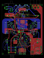
I have layouted and built an amp according to the Project Ember http://www.mediafire.com/view/6l80rilcmqvxxu1/Ember-II_schematic_.pdf with some modification: no auto heater selector, using a 24V AC and regulated using LM317 to 30V, added class A bias for the opamp. It sound fine but i got hiss in one channel: IC3 or the opamp on the left of the picture, the hiss change with tube but not the volume level. At first, i used an external LM2596 for the heater and there is no hiss then i install the onboard heater and hiss appeared so i think it must be some layout prolem. Please take a look at my layout and give me some suggestion, i also attached the eagle layout. Thanks!

Attachments
Hi proid,
well, to me it seems that your layout is insufficient in that respect the LM2576 switcher IC is your source of the problem. You should have a good lock at the datasheet for this IC. There are PCB LAYOUT GUIDELINES on Page 8.
It says:
As in any switching regulator, the layout of the printed circuit board is very important. Rapidly switching currents associated with wiring inductance, stray capacitance and parasitic inductance of the printed circuit board traces can generate voltage transients which can generate electromagnetic interferences (EMI) and affect the desired
operation. As indicated in the Figure 15, to minimize inductance and ground loops, the length of the leads
indicated by heavy lines should be kept as short as possible. For best results, single−point grounding (as indicated) or ground plane construction should be used. On the other hand, the PCB area connected to the Pin 2
(emitter of the internal switch) of the LM2576 should be kept to a minimum in order to minimize coupling to sensitive circuitry. Another sensitive part of the circuit is the feedback. It is important to keep the sensitive feedback wiring short. To assure this, physically locate the programming resistors near to the regulator, when using the adjustable version of the LM2576 regulator.
As far as I see, your problem is that:
1.) You seem to have no ground plane on your PCB. In the good old days one got away with two layer boards without dedicated ground layer . Not anymore, newer technology, e.g. switcher demand solid ground plane under its circuitry ! Criss crossing traces without having a solid ground layer in between is a no go these days !
2.) You did not keep the connections as required short, you made them longer than necessary by unfortunate location of some components also some components for the LM2576.
3.) You OpAmp's and associated traces are too close to your switcher circuit. Signal traces have no business to do in proximity to switcher circuit !
The thing with switchers is, they operate at higher frequency, several hundred kHz up to MHz. Generally the switching signal is not sinoid but has sharp edges which contain even higher frequency spectra. Having no ground plane aids the spreading of the 'love' which your OpAmp happily pick up and amplify for you to enjoy.
I suggest to relocate all the components for the switcher to optimize trace length to be much much shorter. Use a solid ground plane under the switcher circuit. No traces that are not part of the switcher circuit shall come in proximity or cross through that area. Use more than just one via for the Diode and capacitor on the switcher circuit ! The instantaneous currents are quite high. Do not use long skinny traces leading to large capacitors, relocate the capacitor closer such that you have short traces.
As a tip, try re-layout the entire board surrendering the bottom layer as a single solid ground layer and put all signal traces on the top layer. Re-arrainge components clever such that they act as 'bridges' over traces so you can accomplish the required connections. In cases where it is not possible, use short wire bridges. SONY used them extensively too.
Unused board space shall be flooded with copper and connected to ground. Use stitching vias to connect top ground flooding with bottom ground, use several vias, one every 10mm.
I hope I could help you out.
Cheers
Last edited:
To insist on what kct said: the whole ground layout is flawed and the components placement unlogical.
If you're not willing to get new pcb done:
- the lm317 gets its input from the noisiest tracks on the board. Try cutting the input track and solder thick wires from the + leads of the main caps to its input leg.
- the ground track in between the PS and the switcher is shared with the rest of the circuit. As a start, what happens if you cut the bottom track going from the pseudo groundplane under the switcher and solder a thick wire
- And there's no reason I can think of to take the switcher's input from the regulated power. Once again, cut the input + track and wire another wire to the input cap of the switcher.
- keep the extra wires going to the switcher tightly twisted btw.
See on the attached pic.
Attachments
Hi proid,
well, to me it seems that your layout is insufficient in that respect the LM2576 switcher IC is your source of the problem. You should have a good lock at the datasheet for this IC. There are PCB LAYOUT GUIDELINES on Page 8.
It says:
As in any switching regulator, the layout of the printed circuit board is very important. Rapidly switching currents associated with wiring inductance, stray capacitance and parasitic inductance of the printed circuit board traces can generate voltage transients which can generate electromagnetic interferences (EMI) and affect the desired
operation. As indicated in the Figure 15, to minimize inductance and ground loops, the length of the leads
indicated by heavy lines should be kept as short as possible. For best results, single−point grounding (as indicated) or ground plane construction should be used. On the other hand, the PCB area connected to the Pin 2
(emitter of the internal switch) of the LM2576 should be kept to a minimum in order to minimize coupling to sensitive circuitry. Another sensitive part of the circuit is the feedback. It is important to keep the sensitive feedback wiring short. To assure this, physically locate the programming resistors near to the regulator, when using the adjustable version of the LM2576 regulator.
As far as I see, your problem is that:
1.) You seem to have no ground plane on your PCB. In the good old days one got away with two layer boards without dedicated ground layer . Not anymore, newer technology, e.g. switcher demand solid ground plane under its circuitry ! Criss crossing traces without having a solid ground layer in between is a no go these days !
2.) You did not keep the connections as required short, you made them longer than necessary by unfortunate location of some components also some components for the LM2576.
3.) You OpAmp's and associated traces are too close to your switcher circuit. Signal traces have no business to do in proximity to switcher circuit !
The thing with switchers is, they operate at higher frequency, several hundred kHz up to MHz. Generally the switching signal is not sinoid but has sharp edges which contain even higher frequency spectra. Having no ground plane aids the spreading of the 'love' which your OpAmp happily pick up and amplify for you to enjoy.
I suggest to relocate all the components for the switcher to optimize trace length to be much much shorter. Use a solid ground plane under the switcher circuit. No traces that are not part of the switcher circuit shall come in proximity or cross through that area. Use more than just one via for the Diode and capacitor on the switcher circuit ! The instantaneous currents are quite high. Do not use long skinny traces leading to large capacitors, relocate the capacitor closer such that you have short traces.
As a tip, try re-layout the entire board surrendering the bottom layer as a single solid ground layer and put all signal traces on the top layer. Re-arrainge components clever such that they act as 'bridges' over traces so you can accomplish the required connections. In cases where it is not possible, use short wire bridges. SONY used them extensively too.
Unused board space shall be flooded with copper and connected to ground. Use stitching vias to connect top ground flooding with bottom ground, use several vias, one every 10mm.
I hope I could help you out.
Cheers
To insist on what kct said: the whole ground layout is flawed and the components placement unlogical.
If you're not willing to get new pcb done:
- the lm317 gets its input from the noisiest tracks on the board. Try cutting the input track and solder thick wires from the + leads of the main caps to its input leg.
- the ground track in between the PS and the switcher is shared with the rest of the circuit. As a start, what happens if you cut the bottom track going from the pseudo groundplane under the switcher and solder a thick wire
- And there's no reason I can think of to take the switcher's input from the regulated power. Once again, cut the input + track and wire another wire to the input cap of the switcher.
- keep the extra wires going to the switcher tightly twisted btw.
See on the attached pic.
Wow, thank you all for your comment, i though this thread was dead already
 . I initialy layout with a solid bottom ground plane but then i switch to star ground because i think it will improve performance but in the end seem like i did it wrong. Your suggestion is really lighten me, i will try it out but for this:
- the ground track in between the PS and the switcher is shared with the rest of the circuit. As a start, what happens if you cut the bottom track going from the pseudo groundplane under the switcher and solder a thick wire
Do you mean i should cut the trace from the switcher ground plane to the star point and solder a thick wire from ... ?
proid,
try re-layout your board. Before you commit and order the board, post another screenshot of it, this time with your Reference Designation so we can refer to specific components if something still does not seem right.
The Star Layout is ok for low frequency designs, pure Audio, but one has to be very careful when working with higher frequency circuits / design / components e.g. your Switch Mode Power Supply with LM2576. Be absolutely sure that you keep the traces of all components that go with LM2576 to be as short as they can possibly be !
Double or Triple up the Vias for the Inductor, Diode and Capacitors that go with LM2576 !
Keep a healthy distance with all other tracks away from this Switcher Circuit. Consider re-locating your OpAmps circuit further away from the LM2576 circuit.
Here is an article for you to read.
http://ultracad.com/articles/gplane.pdf
Kay
Do you mean i should cut the trace from the switcher ground plane to the star point and solder a thick wire from ... ?
And solder a thick wire from the ground pin of the input capacitor of the lm2596 to the ground pin of the left top cap, like it is shown on the attached pic.
Sorry, I indeed cut a sentence short.
And solder a thick wire from the ground pin of the input capacitor of the lm2596 to the ground pin of the left top cap, like it is shown on the attached pic.
Sorry, I indeed cut a sentence short.
I am expecting that this will not make any difference with the hiss problem whatsoever.
The entire board will have to be re-done, I am afraid.
The lm2576 is quite a slow switcher, at 52khz. While the layout is far from ideal, it might "just work". Worth trying at least.
The weird thing is that the hiss is only in the "left" (wrt the picture) channel. I'd have expected it in the right channel, with the inductor just next to the opamp.
The weird thing is that the hiss is only in the "left" (wrt the picture) channel. I'd have expected it in the right channel, with the inductor just next to the opamp.
- Status
- This old topic is closed. If you want to reopen this topic, contact a moderator using the "Report Post" button.
- Home
- Amplifiers
- Headphone Systems
- Hissing problem of a hybrid amp