..just want to share my amp schematic. Here is

Another attached file is a sprint layout 6 board. R2 is better must be a trimmer that should be used to set preout voltage offset (6.7V with 12V power is best one).
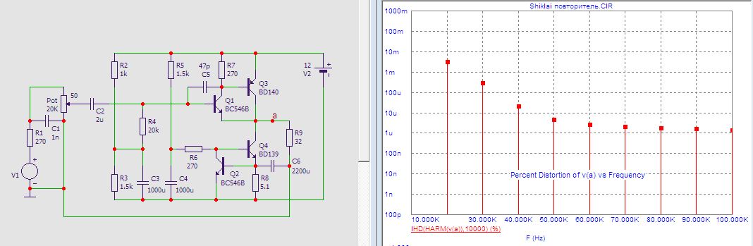
While having only 7 transistors/channel without opamp it has voltage gain 3 and gives ~0.001% THD on 3Vp/64Ohm load and most of this is 2nd harmonic. Also it features almost constant PSU drain current (about 140mA/channe) that minimizes power source effect on sound, so only capacitors that mostly affect sound are in- and out- decoupling caps. Also it doesn't requre stabilized power and works from 12V or more voltage.. Actually - the more voltage it powered - the more output voltage (and less distorted on same voltage) it will produce.. Until something will burn out🙂
Another attached file is a sprint layout 6 board. R2 is better must be a trimmer that should be used to set preout voltage offset (6.7V with 12V power is best one).
While having only 7 transistors/channel without opamp it has voltage gain 3 and gives ~0.001% THD on 3Vp/64Ohm load and most of this is 2nd harmonic. Also it features almost constant PSU drain current (about 140mA/channe) that minimizes power source effect on sound, so only capacitors that mostly affect sound are in- and out- decoupling caps. Also it doesn't requre stabilized power and works from 12V or more voltage.. Actually - the more voltage it powered - the more output voltage (and less distorted on same voltage) it will produce.. Until something will burn out🙂
Attachments

Last edited:
I'm not 100% agree with "minimal NFB" in the name. While it has no global feedback loop, it has two local-ish loops with reasonable amount of loop gain.
2Sergey888 thats why its 'minimal NFB' but not zero-NFB
Also there is some philosophical point that output feedback doesn't a signal feedback, its actually transistors mode feedback, that stabilizes collector current on 100mA level that actually provides linearity (and if load current will achieve this value - distortions will quickly go higher.. but 100mA limit must be enough for most cases).
2ShadowMike 1mF = 1000uF. So output cap is 3300uF (note that relay protection to prevent on/off voltage peaks due to capacitor (dis)charge is recommended, especially for turning off)
Also there is some philosophical point that output feedback doesn't a signal feedback, its actually transistors mode feedback, that stabilizes collector current on 100mA level that actually provides linearity
That's local feedback. It provides AC feedback. Feedback is feedback.
What you have is a two stage amplifier.
Member
Joined 2009
Paid Member
Is the output inductor required, I don't see them often on headphone amplifier schematics, or maybe I haven't been looking properly ?
Its capacitive load decoupling, without it and without R14/C9 I saw that output oscillates on very high frequency (about 10MHz) when long cable connected to output.
Oscillation stops if L1/R17 added or if R14/C9 added. I included both in schematics just to be sure 🙂.
This components should not make things worse in terms of audio.. Its still fast enough: only about 0.75 degree phase error at 20Khz
Oscillation stops if L1/R17 added or if R14/C9 added. I included both in schematics just to be sure 🙂.
This components should not make things worse in terms of audio.. Its still fast enough: only about 0.75 degree phase error at 20Khz
Last edited:
However note that most of other headphone amplifiers has a resistor on output to provide stability. Probably such solution also can be used here, but damped induction filter gives almost zero output impedance in sound range unlike single resistor.
I winded output inductor as 12 windings of D=1.3mm wire on 12mm cylinder. With 1mm wire there must be 10 windings on same 12mm.
I winded output inductor as 12 windings of D=1.3mm wire on 12mm cylinder. With 1mm wire there must be 10 windings on same 12mm.
Last edited:
Cool little amplifier, that one (not in the literal sense obviously, given the current draw 😉). Gives the old grey matter a bit of a workout.
Is Q3, Q5 = BD140 deliberate? That type would seem to be a tad slow at only ~2 mA Ic (Q3) - the On Semi datasheet says Cob at 6 V would be 30-35 pF, a lot higher than for typical small-signal parts, which would certainly take its toll on high-frequency distortion as well, in addition to already lower loop GBW.
I imagine gain stage distortion could be reduced further by better matching of the "folded-open differential amplifier" stage transistors, Q1 and Q2. I should really give this VFB topology a closer look and compare it to, say, a classic CFB approach with the same number of transistors.
While an output inductor is certainly commendable, I would have tried a Zobel (RC to output ground) first, which is far simpler to implement. Both can also be used together, as done in many speaker power amps.
Actually a simple circuit at high current like that should be able to work without any fancy measures against capacitive loading. Maybe adding a capacitor across B-C of Q5 for loop gain compensation would allow reducing C10 and make things a little better-behaved? I'm thinking this because the troublesome characteristic in emitter followers WRT stability is the 1st-order beta/hFE dropoff (which likes to transform inductive source impedances into nasty things thanks to its 90° phase shift), and C10 would be making Q6 a fair bit slower.
And I think it's obvious, but of course a push-pull output stage is not SE. 😉
Q3/Q5 used BD140 cuz in the load short-circuit condition they must deal with quite big currents (R13 also used to protect Q5 in such case but still base current in short circuit condition is matter of 0.1..0.3A that is too huge for most of small signal transistors).
Also when played on breadboard I did some experiments with transistors and found that BD140 you mentioned can be replaces with KTA1023. No measurable thing get worse with it, but actually nothing become better. To achieve best linearity that transistors must have flat Vbe(Ic) characteristics and BD140 appeared not bad in that.
About why and how it works. The idea of whole circuit is to set transistors to work with smallest collector current deviations. Actually both parts (voltage amplifier and output) are derived from well known 2 transistors current source schema:
 that has 'embedded' transistor in the emitter of Q2 and R2 replaced with additional current source to improve linearity. When considering output stage of my circuit that additional transistors works as emitter follower and its surroundings force its collector current to remain same (almost same in reality) value. There is another variation of same idea:
However while that another variation is simplier by one transistor it has problems with grounding, specially if you have to implement 2 stereo channels with same ground. The idea of that another schema is pretty the same - follower with stable collector current, but unlike my schema - the current sensing resistor (r8) is not in the collector, but in the emitter circuit, but after AC+DC load.
So I'm not very far from truth if tell that output stage doesn't have NFB. It has feedback, but its not a output-input feedback, its a current-source feedback that provides near-to-ideal current mode for transistor follower.
The input stage of my circuit also works in the stabilized current condition but actually it has obvious feedback, and even that feedback can be switched from input to output stage effectively making whole schema to usual global NFB amp, but it would be not so interesting then 🙂
Also due to constant-current mode of output stage (and due to R15) - it appears as constant-current sink for input stage, eliminating need for additional transistor that will be necessary if input stage will be used without such output.
And I don't agree with push-pull. Its not 'more' push-pull than usual follower loaded to constant emitter current sink. So if such followers are sometimes called as 'follower with active load' so mine is probably 'follower with hyper-active load' 🙂
Also when played on breadboard I did some experiments with transistors and found that BD140 you mentioned can be replaces with KTA1023. No measurable thing get worse with it, but actually nothing become better. To achieve best linearity that transistors must have flat Vbe(Ic) characteristics and BD140 appeared not bad in that.
About why and how it works. The idea of whole circuit is to set transistors to work with smallest collector current deviations. Actually both parts (voltage amplifier and output) are derived from well known 2 transistors current source schema:
However while that another variation is simplier by one transistor it has problems with grounding, specially if you have to implement 2 stereo channels with same ground. The idea of that another schema is pretty the same - follower with stable collector current, but unlike my schema - the current sensing resistor (r8) is not in the collector, but in the emitter circuit, but after AC+DC load.
So I'm not very far from truth if tell that output stage doesn't have NFB. It has feedback, but its not a output-input feedback, its a current-source feedback that provides near-to-ideal current mode for transistor follower.
The input stage of my circuit also works in the stabilized current condition but actually it has obvious feedback, and even that feedback can be switched from input to output stage effectively making whole schema to usual global NFB amp, but it would be not so interesting then 🙂
Also due to constant-current mode of output stage (and due to R15) - it appears as constant-current sink for input stage, eliminating need for additional transistor that will be necessary if input stage will be used without such output.
And I don't agree with push-pull. Its not 'more' push-pull than usual follower loaded to constant emitter current sink. So if such followers are sometimes called as 'follower with active load' so mine is probably 'follower with hyper-active load' 🙂
Attachments

Last edited:
And forgot to answer about Zobel. RC used to isolate compensate load's inductance. Its not issue here - in case of headamp its usually necessary to compensate load's capacitance and RC to ground will not change anything there, that actually I saw on board. Also actually circuit seems stable with inductive load, the issue only with capacitive one.
Usual ways to compensate load capacitance - either serial resistance on output either serial resistance paralleled with inductance. First solution also increases output impedance that commonly used to limit short circuit current but this is not issue her - this schema has own short-circuit current limiters, so no need to defeat output impedance and RL is better solution here than simple R IMHO.
Usual ways to compensate load capacitance - either serial resistance on output either serial resistance paralleled with inductance. First solution also increases output impedance that commonly used to limit short circuit current but this is not issue her - this schema has own short-circuit current limiters, so no need to defeat output impedance and RL is better solution here than simple R IMHO.
I'd say this is nothing that some strategically placed resistors in series with the emitters of Q2, Q3, Q5 couldn't fix though...Q3/Q5 used BD140 cuz in the load short-circuit condition they must deal with quite big currents (R13 also used to protect Q5 in such case but still base current in short circuit condition is matter of 0.1..0.3A that is too huge for most of small signal transistors).
You could also increase loop gain by replacing R5 with a current source (flatten out across the audio band with a parallel R if need be).
A while back there was a design presented here that yours reminded me of; look, I found it (there are some upsides to being a browser tab messie at least): Gilberd headphone amplifier
The input stage should look familiar...
Last edited:
Resistor in base is quite a strategical place. Sure, its always possible to try to find better alternative🙂, but.. Putting resistors between emitters of Q2/Q3 (both as Q6/Q7) will limit maximum amplitude (that will reduce linearity on low amplitude too).
Putting resistor into emitter of Q3/Q6 also will degrade linearity even more cause linearity achieved due to Q1-Q2 and Q6 collector currents stabilized with Q3 and Q5 respectively. Laters keep current so voltage drop on R5 and R16 will be on the edge of their opening. Putting resistor into current-sensing Q's emitter will blur that edge and thus Q1-Q2/Q6 collectors currents deviations will raise dramatically. More current deviation on signal-carring transistors will cause more distortion cuz gain and (especially) Vbe of transistors directly depend on their's collector current.
Also thats why Gilbert's amplifier input stage is not similar actually. There is not current stabilization loop, there is loop with opamp, but its integrator that doesn't do that on audio frequency. However about integrator - it allowed Gilbert amplifier to work without output capacitor, however since its schema doesn't sink stable current and doesn't have NFB - output signal still affected by capacitors, or more exactly - by power supply and its capacitors.
In my schema the only electrolytic capacitor that affect sound - C11, because whole circuit's current consumption is almost not depends on signal. More precisely - with signal amplitude 3Vp on 64 ohm load, so when load's current amplitude is approx 46mA - the whole circuit current deviation amplitude is only 1.3mA. So.. there is another simple way to protect against short circuit overcurrent - just put polyfuse around whole circuit 🙂 and rather small electrolytic cap after - just to feed that 1.3mA deviations.
BTW also there is way to get rid of output cap and even more stabilize whole current - just build a bridge 🙂 It requires to make signal inversion somehow and.. its theoretically possible with similar technique:
http://www.diyaudio.com/forums/attachment.php?attachmentid=491448&stc=1&d=1435774444
Here I made simple signal invertor with similar 3-transistors current-stabilized ring on input and used depletion mode FET on one of the output stages to get some voltage level-up. It doesn't have any voltage amplification except of bridge-caused doubling. V3 must be some stabilized reference voltage source and R1 must be adjustable to adjust outputs DC offset to zero. Or R1 can be fixed and the DC fine-tuning can be done by V3 adjusting. Theoretically it should work and theoretically it should not require integrator even if whole voltage source will not be stabilized cuz all voltage levels are defined by resistors relations and Vbe dropouts, and laters are depend on collector currents that are stabilized. I told theoretically - cuz never tried this bridge schema. Only simulated. I suspect in practice it will require more corrections for stability, especially those part that contains FET.
Attachments

Last edited:
- Status
- Not open for further replies.
- Home
- Amplifiers
- Headphone Systems
- single-ended (hope:) ) headphone amplifier with minimal NFB and low THD