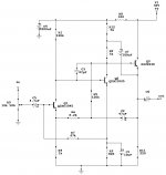
I would like to share a headphone amp design that I have been working on for the past few weeks. Since I only recently had a need to use hp's this is my first go at a design for them. Since you can basically throw a rock anywhere on the net and find opamp designs, I wanted something discrete and a topology rarely seen in today's designs. After digging through tons of old schematics, I kept seeing this topology used in low level gain stages starting all the way back to mid 50's when transistors first became available and then basically disappearing after the early 70's. Douglas Self called it a 2-transistor shunt-feedback amplifier Discrete design: More on 2-transistor shunt-feedback amplifiers So after some simulating, prototyping, tweeking, and some probably not so accurate measuring, I found it to have very good performance. This design of course won't be for everyone (eek look at all those capacitors) but I find it enjoyable to listen to for hours. It's simplicity to build also made it fun to tweek and experiment. So anyway I give you what I am calling the Classic-50mW, the classic part being obvious and 50mW since this is the power it can give into 32-600 ohm hp's.
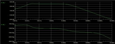
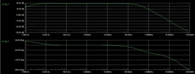
Attached is schematic, frequency sims (open and closed loop), and in the zip is a .htm file generated by RMAA6 containing measurements of soundcard loopback alone compared with the amplifier loaded with 32 ohm inserted into the loopback. It's rather obvious the soundcard is the real limiting factor here.
Attached is schematic, frequency sims (open and closed loop), and in the zip is a .htm file generated by RMAA6 containing measurements of soundcard loopback alone compared with the amplifier loaded with 32 ohm inserted into the loopback. It's rather obvious the soundcard is the real limiting factor here.
Attachments
Last edited:
Oops looks like I messed up on the Comparison archive and left out the graphs.
thank you jerluwoo for the additional information on this design!
how would you describe it's sound?
i'm trying to adapt it to 12v supply, that's the only PS i have right now, and also ideally have it driving a small speaker for desktop use, hope you wouldn't mind.
the various feedback paths get everything interconnected, and i'm have a hard time getting it all working together, the THD i get now is way worse than yours, around 0.74% as it is now.
any general advices on how to adapt it to 12v supply?
what kind of collector current should i shoot for for each transistor?
also i'm curious about how one design and simulate speed, could you give a brief lecture on that? thank you!
Last edited:
Are you using the above circuit or the one from here?the various feedback paths get everything interconnected, and i'm have a hard time getting it all working together, the THD i get now is way worse than yours, around 0.74% as it is now.
TBH that's the kind of result I'd expect for a 4-transistor AB amp driving a speaker at any kind of power. If that's an unloaded result, however, chances are your operating point is off. The output probably isn't anywhere close to half supply.
Even if you do get the operating point right, you can still expect to see appreciably worse distortion at a 12 V supply vs. 32 V. Either you leave the resistors as-is, which reduces standing currents significantly, or you decrease them as needed, in which case they make a worse current source approximation, and you may need to employ "real" current sources instead. This circuit also has a reasonably high output impedance pre-feedback due to the bootstrap, so the loop gain gained by that is drained immediately if you connect a low-impedance load (hence also why the speaker version is not bootstrapped, I presume - it would require one more current gain stage).
But yes, these circuits with multiple DC feedback paths tend to be real head-scratchers. Part values are typically optimized iteratively, going from desired voltages and device currents.
the various feedback paths get everything interconnected, and i'm have a hard time getting it all working together, the THD i get now is way worse than yours, around 0.74% as it is now.
The voltage at Q3 emitter is undoubtedly lower than what it should be, reducing available current output.
i'm trying to adapt it to 12v supply, that's the only PS i have right now, and also ideally have it driving a small speaker for desktop use, hope you wouldn't mind.
Change value of R11 to 100 ohms. Change the value of R3 by increasing in value (1k 1.2k 1.3k etc. or replace with a multi-turn pot) until you get 6 volts at the emitter of Q3. Recalculate the value of C1= 1/(2*pi*20*R3) . Distortion will still be higher than with the higher B+.
Attached is test I did with 8ohm speakers at 10mW. Loud enough for close field listening with sensitive speakers. I built a second version also for speakers by changing only 2 components, but, this is the headphone section and not the proper place.
Hi. Is the input a 10k pot??
Yes a dual audio taper.
Attachments
Last edited:
Are you using the above circuit or the one from here?
I have not built or tested the a/b circuit, it was just an example based on this circuit. I am confident it will work well enough for a learning tool. Certainly not hifi in any respect.
Even if you do get the operating point right, you can still expect to see appreciably worse distortion at a 12 V supply vs. 32 V. Either you leave the resistors as-is, which reduces standing currents significantly, or you decrease them as needed, in which case they make a worse current source approximation, and you may need to employ "real" current sources instead. This circuit also has a reasonably high output impedance pre-feedback due to the bootstrap, so the loop gain gained by that is drained immediately if you connect a low-impedance load (hence also why the speaker version is not bootstrapped, I presume - it would require one more current gain stage).
Correct on all except that the circuit will not function with a current source load on Q2. Output impedance is ~6 ohms. If you look at the test on 8ohm load from previous post you will see a rise in output in the bass on the frequency plot. This is where the output capacitor impedance began to rise creating a higher load value.
But yes, these circuits with multiple DC feedback paths tend to be real head-scratchers. Part values are typically optimized iteratively, going from desired voltages and device currents.
I had to make a few compromises on device operating points so it would provide the stated power on a wide range of headphone impedances.
Last edited:
... After digging through tons of old schematics, I kept seeing this topology used in low level gain stages starting all the way back to mid 50's when transistors first became available and then basically disappearing after the early 70's. ...
Interesting, not least because it also uses my favourite small-signal transistor - the 2sc1845. However, you can probably get better sonics and performance with a modified c.1969 JLH 4-BJT Class-A with a PNP input stage - it has about the same parts count as the 3-BJT schematic you've posted. The JLH can also be made to run comfortably on lower rails like 9 to 12V, single-supply.
What do cap 5 and 6 do??
These are signal coupling capacitors. C5 value should not be changed as it is calculated for a specific roll off and phase in conjunction with R7,R3,and C1. C6 can be chosen for the intended load. I prefer to calculate it as having an impedance 1/10 of the load at 20hz rather than for F3 at a specific frequency to maintain a minimum damping factor. This will make it much larger than what would usually be used, as an example, for 32 ohms I use 2,200uF.
Are you using the above circuit or the one from here?
TBH that's the kind of result I'd expect for a 4-transistor AB amp driving a speaker at any kind of power. If that's an unloaded result, however, chances are your operating point is off. The output probably isn't anywhere close to half supply.
Even if you do get the operating point right, you can still expect to see appreciably worse distortion at a 12 V supply vs. 32 V. Either you leave the resistors as-is, which reduces standing currents significantly, or you decrease them as needed, in which case they make a worse current source approximation, and you may need to employ "real" current sources instead. This circuit also has a reasonably high output impedance pre-feedback due to the bootstrap, so the loop gain gained by that is drained immediately if you connect a low-impedance load (hence also why the speaker version is not bootstrapped, I presume - it would require one more current gain stage).
But yes, these circuits with multiple DC feedback paths tend to be real head-scratchers. Part values are typically optimized iteratively, going from desired voltages and device currents.
i'm using the one posted here, in this thread.
thanks a lot sgrossklass for your advices/tips/comments, very useful and helpful to me indeed!
The voltage at Q3 emitter is undoubtedly lower than what it should be, reducing available current output.
Change value of R11 to 100 ohms. Change the value of R3 by increasing in value (1k 1.2k 1.3k etc. or replace with a multi-turn pot) until you get 6 volts at the emitter of Q3. Recalculate the value of C1= 1/(2*pi*20*R3) . Distortion will still be higher than with the higher B+.
Attached is test I did with 8ohm speakers at 10mW. Loud enough for close field listening with sensitive speakers. I built a second version also for speakers by changing only 2 components, but, this is the headphone section and not the proper place.
thank you for the help!
Hi there !! I know is bit old thread, just a couple of questions. What is the voltage gain of this amp? What is the quiescent current of the circuit ? Let's say driving it's input at a typical CDP 2V output signal on the higher impedance , due to AC coupling directly from I/V converter. Can this amp be used as a line buffer and what would be the voltage swing at it's output by applying a 600 ohm load?I would like to share a headphone amp design that I have been working on for the past few weeks. Since I only recently had a need to use hp's this is my first go at a design for them. Since you can basically throw a rock anywhere on the net and find opamp designs, I wanted something discrete and a topology rarely seen in today's designs. After digging through tons of old schematics, I kept seeing this topology used in low level gain stages starting all the way back to mid 50's when transistors first became available and then basically disappearing after the early 70's. Douglas Self called it a 2-transistor shunt-feedback amplifier Discrete design: More on 2-transistor shunt-feedback amplifiers So after some simulating, prototyping, tweeking, and some probably not so accurate measuring, I found it to have very good performance. This design of course won't be for everyone (eek look at all those capacitors) but I find it enjoyable to listen to for hours. It's simplicity to build also made it fun to tweek and experiment. So anyway I give you what I am calling the Classic-50mW, the classic part being obvious and 50mW since this is the power it can give into 32-600 ohm hp's.
Attached is schematic, frequency sims (open and closed loop), and in the zip is a .htm file generated by RMAA6 containing measurements of soundcard loopback alone compared with the amplifier loaded with 32 ohm inserted into the loopback. It's rather obvious the soundcard is the real limiting factor here.
Thanks a lot for your guidance
Andreas
Idle current for the entire circuit would be 73-75 mA per channel. Gain is R6/R4 or ~ 8. 700mV rms input will give 6V rms out into 600 ohms. It is designed to deliver 50mW into 32-600 ohms. It should have no trouble as a line driver.
Thanks for you prompt response. This circuit is gorgeous due to single voltage rail and premium transistors used. Can I decrease the ratio of R6/R4 to lower the voltage gain? (e.g. setting R6 to 3K7) If so, would be any consequences to the other parts operating points?
Last but not least, can I pick your circuit values and voltages to implement the Douglas Self 2 transistors shunt feedback amplifier by applying the c1845 in both stages ? Collector values of 5K and 5K can be OK for Q1 stage? What value should be the shunt feedback resistor (R5) then?
I need to create a simple linear buffer stage, providing a voltage gain no more than 3 and to avoid several feedback paths and the essential coupling capacitors..The 70mA load per channel "smells" deep ClassA operation, and I should need an additional tube rectifier to feed them both. But if this worths the sonics, I guess I can manage.
I hope to make sense.
Thanks again Andreas
")
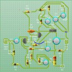
Simple pc-board layout and gerbers.
*note. Q1-2 are set up for BC and 2N type pinouts. 2SC types can be fitted with attention to pin placement. Q3 should be fine for all TO-220 pinouts.
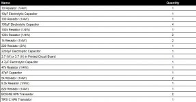
Bill of materials for single channel. Transistors can be nearly any type with Q1-2 minimum 40V Vce, 300 Hfe. Q3 minimum 40V Vce, 100 Hfe.
*note. Q1-2 are set up for BC and 2N type pinouts. 2SC types can be fitted with attention to pin placement. Q3 should be fine for all TO-220 pinouts.
Bill of materials for single channel. Transistors can be nearly any type with Q1-2 minimum 40V Vce, 300 Hfe. Q3 minimum 40V Vce, 100 Hfe.
Attachments
Last edited:
- Status
- This old topic is closed. If you want to reopen this topic, contact a moderator using the "Report Post" button.
- Home
- Amplifiers
- Headphone Systems
- Classic-50mW