Is this too simple:
sims very nice with the right bias
An externally hosted image should be here but it was not working when we last tested it.
sims very nice with the right bias
too big mosfet - more Coss + Crss parasitic Q to drive to full Vout than most ES headphones
too little bias too 400V/200kOhm = 2 mA, which leads to
too slow with ~ 3 kHz pole, with
too short a feedback loop so the pole is open loop - directly rolls off the audio
there are a few sub 1 A high V mosfet being made, IXYS http://ixapps.ixys.com/DataSheet/DS98809C(IXTP-U-Y01N100D).pdf is a better fit with order of magnitude smaller parasitic C
Last edited:
This started as a piezo driver project for a mechanical actuator, and morphed into an amplifier as I have a bunch of IRFPG40's left over from a HV power supply loosely based upon Horowitz and Hill. The OPA1632 is a nice chip for deriving the 2 out of phase signals.
The device you site is a depletion mosfet, so will require a bit more work --
The device you site is a depletion mosfet, so will require a bit more work --
depletion mode isn't really a big difference - just the Vgs DC component changes, but it does open the possibility of a self biased "srpp derived" modulating ccs
the opa1623 does look good - you can extend the SuSy feedback to the output with some compensation - my sims show a large SuSy "extra" distortion cancellation when the diff output is measured
ES headphones seem to use gnd referenced stator drive and bias V is applied to the membrane - I think this is motivated by safety concerns
so you usually see DC blocking output C with single supply ES headphone amp designs
and then you get the complaints that the C hurts the sound
if you like enhancement mode - another device I have on order: N-Channel Power MOSFET, 1500V, 0.1A, 150?, TO-220F-3FS
if you want to see what's being done in ES headphone amps its probably worth looking for Kevin Gilmore's pages, projects, posts - some found at Head-Fi.org, more at Do It Yourself - www.Head-Case.org
Class A ES headphone amps seem to typically run 5-10 mA bias current
Class A ES headphone amps seem to typically run 5-10 mA bias current
Hi,
just found this:
1-kV Piezo Amplifier Keeps Cost, Noise Low | Components content from Electronic Design
Seems nice and easy to build, a simulation in LTSpice shows that almost any medium power, high voltage npn transistor can be used as well (commonly used in CRT screens...).
Just omit everything after R5 and duplicate the rest for BTL (invert one input, too). The CCS (Q2, R2 and the 9V battery) could be improved though...
Seems almost too simple Do I miss anything?
Best regards
just found this:
An externally hosted image should be here but it was not working when we last tested it.
1-kV Piezo Amplifier Keeps Cost, Noise Low | Components content from Electronic Design
Seems nice and easy to build, a simulation in LTSpice shows that almost any medium power, high voltage npn transistor can be used as well (commonly used in CRT screens...).
Just omit everything after R5 and duplicate the rest for BTL (invert one input, too). The CCS (Q2, R2 and the 9V battery) could be improved though...
Seems almost too simple
Best regards
Do I miss anything?
I saw that design, or one similar in EDN -- you have to bias up the MOSFET driven by the OP27 to about 4 volts to get it to go.
As JCX points out, a depletion mosfet allows the possibility of self-biasing. In some experimenting, however, i can't get it to operate as "linearly" as I would like.
Schematic in post #1 seems to run a common source amplifier + source follower buffer with no global negative feedback. So whatever lousy PSRR you get from R1+R2, is not reduced by the feedback factor. post#7 seems to eliminate this deficiency.
If it's challenging to make a low-Zout, low-noise, +15VDC supply, it's probably even harder to do the same at +400VDC.
Edit- whoops! If the headphone element is driven push-pull and if the two NMOS amps+buffers are very well matched, then injected supply noise is cancelled at the driver.
Vdriver = (LeftHandSide + SupplyNoise) - (RightHandSide + SupplyNoise) = LeftHandSide - RightHandSide.
Last edited:
I saw that design, or one similar in EDN -- you have to bias up the MOSFET driven by the OP27 to about 4 volts to get it to go.
As JCX points out, a depletion mosfet allows the possibility of self-biasing. In some experimenting, however, i can't get it to operate as "linearly" as I would like.
If you mean Q1, there is absolutely no problem, just add an offset to the input signal of OP27.
Q2 is kind of a problem indeed. A depletion FET is one solution, another (more obtainable one) is a simple two-transistor-CCS.
My simulation looks fine, soon I will solder a prototype to test that circuit
Last edited:
Hi,
...a simulation in LTSpice shows that almost any medium power, high voltage npn transistor can be used as well (commonly used in CRT screens...)
...Seems almost too simpleDo I miss anything?
Best regards
posting the .asc?
I expect it to be rather poor in crossover/commutation
at headphone power levels Class A is common - at ES V levels and biasing for 20 kHz C load the power does become excessive but is a pretty universally accepted cost of these amps
Sure:
View attachment ESL.asc
Tell me what you think about it, I haven't had the time to build it up yet.
The 70Ohm resistors adjust the quiescent current (the lower the resistance the better the rise time but the more heat).
In the CCS section I chose a BF821 for the "power" transistor... not suitable but this is just a generic part, almost everything
that's capable of >1.5W and withstands the supply voltage should work.
Had some spare time and soldered the circuit for a first test.
I have made some minor changes to the .asc-file, so this is the current schematic:
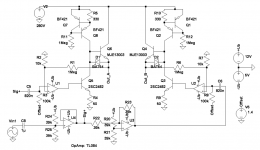
To summarize my results: there's music playing out of my ESL
But there's also some serious oscillation in there I have to fix in the next version Maybe I should at least separate the two driver OpAmps
(and replace them by R2R types, so -Ub isn't needed anymore) in order to minimize capacitive coupling.
We'll see...
I have made some minor changes to the .asc-file, so this is the current schematic:

To summarize my results: there's music playing out of my ESL
But there's also some serious oscillation in there I have to fix in the next version
(and replace them by R2R types, so -Ub isn't needed anymore) in order to minimize capacitive coupling.
We'll see...
At last, my circuit's working fine 
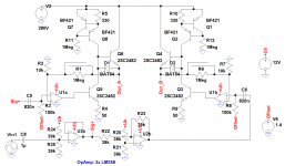
I exchanged the TL084 with two LM358 and optimized the two capacitors across R1 and R6, so there's almost no oscillation present anymore.
The C's values are a bit critical, that's why my first circuit didn't work fine.
The schematic used:
And a photograph of my prototype:
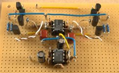
There you see the two capacitors made of twisted wires.
By cutting them while oscilloscoping the output signal you can easily achieve the point of least oscillation.
I had a short listening session with my unfinished headphones, though they are in need of some equalization, there is no audible distortion
added by the circuit. Though the bias voltage of about 140V (with the diaphragm at GND) is enough to listen at home,
I added another -270V to the diaphragm (results in approx. 400V). Now, that's an improvement and nearly fun to listen to
I have to do my headphones...
Best regards
I exchanged the TL084 with two LM358 and optimized the two capacitors across R1 and R6, so there's almost no oscillation present anymore.
The C's values are a bit critical, that's why my first circuit didn't work fine.
The schematic used:

And a photograph of my prototype:

There you see the two capacitors made of twisted wires.
By cutting them while oscilloscoping the output signal you can easily achieve the point of least oscillation.
I had a short listening session with my unfinished headphones, though they are in need of some equalization, there is no audible distortion
added by the circuit. Though the bias voltage of about 140V (with the diaphragm at GND) is enough to listen at home,
I added another -270V to the diaphragm (results in approx. 400V). Now, that's an improvement and nearly fun to listen to
I have to do my headphones...
Best regards
- Status
- This old topic is closed. If you want to reopen this topic, contact a moderator using the "Report Post" button.
- Home
- Amplifiers
- Headphone Systems
- Too simple MOSFET ESL amplifier