good stuff -> opa140 / opa2140 / opa4140
Sergey888 - I finally got a chance to look into your OPA140/2140/4140 suggestion back in post #12. Now that chip is fantastic for this project! Great find. Still JFET input with pico-amps of input bias current, won't load the O2's pot or cause any significant drop across the 40.2K resistor, AND still has ultra-low output offset voltage. 120uV, just like the OPA827. Finding that combination is a real trick. I've found several op amps with low Vos, like the OPA211, but high (bipolar) input bias current. Then a bunch of FET input op amps that have high input offset voltages.
I see that TI is pitching the OPA140 group specifically for battery operatated equipment like this project, since it only has 2mA or so per amplifier. The NJM4556A in the O2 was listed at 9-12mA total, and the LME49600 in low BW mode is 7mA, so the OPA141+LME49600 would be 9mA vs. a maximum of 6mA per amp for the NJM4556A, only about 50% more. Much lower draw than the OPA827+LME49600 pair.
I see the noise figures on the OPA140/2140 are just a hair worse, 5nV/sqrt(Hz) vs. 4 for the OPA827, might not even be audible. A reasonable trade-off for increaed battery life. Same with THD+N. At 20kHz the 140/2140 it 0.0004% vs. 0.0002% for the OPA827.
Plus the OPA140, the single version, is pin compatible with the OPA827 and would work in this same board layout! In fact, I'll get a few in from Mouser and build one board up with OPA827s and another with OPA140s. The 2140 would save space and eliminate one chip, still SOIC-8, but I kind of like being able to use either the 827s (or 627's - those would work too for more $$$) or the 140s in the dual single layout.
So now there can be two different builds on the same board. OPA827+LME49600 for the "high performance" build with higher current draw but a tad less noise and THD, or the OPA140+LME49600 for the "high battery life" build.
You are right about C5 and C11. Right two traces but wrong place on the traces. Given the high bandwidth of the chips those were in case of very high frequency ocillations when the traces look like inductors. But isn't going to do much good over on the LME49600 end rather than the OPA827 end. I couldn't find a place to fit the caps, then saw that spot by the 49600, but didn't go back and think through the circuit. Oh well, the hope/expectation is those won't be needed anyway given the short, wide, traces.")
I also settled on the decoupling method in fig. 3 in this Analog Devices app note on layouts for dealing with falling chip PSRR vs. frequency:
http://www.analog.com/static/imported-files/tutorials/MT-043.pdf
Hence the (relatively) low ESR 47uF solid tantalums in the middle, with the COG ceramics up at the chip leads, plus the 4.7uF solid tantulums in parallel on the LME49600 leads from that chip's data sheet. Lol - after all that hopefully it will be stable. I'm going to drop 1nF and 2nF across the headphones for a reactance test.
Sergey888 - I finally got a chance to look into your OPA140/2140/4140 suggestion back in post #12. Now that chip is fantastic for this project! Great find. Still JFET input with pico-amps of input bias current, won't load the O2's pot or cause any significant drop across the 40.2K resistor, AND still has ultra-low output offset voltage. 120uV, just like the OPA827. Finding that combination is a real trick. I've found several op amps with low Vos, like the OPA211, but high (bipolar) input bias current. Then a bunch of FET input op amps that have high input offset voltages.
I see that TI is pitching the OPA140 group specifically for battery operatated equipment like this project, since it only has 2mA or so per amplifier. The NJM4556A in the O2 was listed at 9-12mA total, and the LME49600 in low BW mode is 7mA, so the OPA141+LME49600 would be 9mA vs. a maximum of 6mA per amp for the NJM4556A, only about 50% more. Much lower draw than the OPA827+LME49600 pair.
I see the noise figures on the OPA140/2140 are just a hair worse, 5nV/sqrt(Hz) vs. 4 for the OPA827, might not even be audible. A reasonable trade-off for increaed battery life. Same with THD+N. At 20kHz the 140/2140 it 0.0004% vs. 0.0002% for the OPA827.
Plus the OPA140, the single version, is pin compatible with the OPA827 and would work in this same board layout! In fact, I'll get a few in from Mouser and build one board up with OPA827s and another with OPA140s. The 2140 would save space and eliminate one chip, still SOIC-8, but I kind of like being able to use either the 827s (or 627's - those would work too for more $$$) or the 140s in the dual single layout.
So now there can be two different builds on the same board. OPA827+LME49600 for the "high performance" build with higher current draw but a tad less noise and THD, or the OPA140+LME49600 for the "high battery life" build.
You are right about C5 and C11. Right two traces but wrong place on the traces. Given the high bandwidth of the chips those were in case of very high frequency ocillations when the traces look like inductors. But isn't going to do much good over on the LME49600 end rather than the OPA827 end. I couldn't find a place to fit the caps, then saw that spot by the 49600, but didn't go back and think through the circuit. Oh well, the hope/expectation is those won't be needed anyway given the short, wide, traces.
I also settled on the decoupling method in fig. 3 in this Analog Devices app note on layouts for dealing with falling chip PSRR vs. frequency:
http://www.analog.com/static/imported-files/tutorials/MT-043.pdf
Hence the (relatively) low ESR 47uF solid tantalums in the middle, with the COG ceramics up at the chip leads, plus the 4.7uF solid tantulums in parallel on the LME49600 leads from that chip's data sheet. Lol - after all that hopefully it will be stable. I'm going to drop 1nF and 2nF across the headphones for a reactance test.
Last edited:
I didn't tell you that OPA140 is a brother of OPA1641 with, i guess, slightly different front end bias current and a bit lager area of input transistors. So all worries about how it sounds are relevant here But honestly I would not worry about.
I would not bother with C0G/NP0 cap on supply lines. Capacitor linearity is irrelevant here. X7R/X5R will work as good or even better, because you''l be able to place larger value capacitor, or use smaller capacitor with the same value and put it closer to a consumer.
But honestly I would not worry about.I would not bother with C0G/NP0 cap on supply lines. Capacitor linearity is irrelevant here. X7R/X5R will work as good or even better, because you''l be able to place larger value capacitor, or use smaller capacitor with the same value and put it closer to a consumer.
agdr
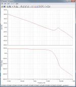
LME49600 has an ugly peak around 100MHz. It look bad in combination amost with any opamp if you do not put any additional freq compensation around.
That is what it looks like with OPA140. It is not acceptable. It gets even worse if you use wide bandwight mode.
I'm playing with few different variants in simulator. Nor sure which on is the way to go so far.
Attachments
agdr
Probably the simplest way to make nice is to put around 15pF capacitor from output of opamp to its inverting input and 1k resistor from LME output.
If you want to make it second order, just replace 15pF capacitor with two 33pF in series and put something like 3.3k resistor from the middle point to the ground. But advantage is not as big, ~6dB in audio band.
Sergey888 - good find about the high frequency gain spike. Looks like the gain is heading back toward unity at 80MHz or so. I'll add the 15pF and 1kHz, circuit below. This V1.0 PCB is just a prototype anyway so I'll cut / jumper / hand-solder parts as needed to get those caps and resistors in the right place.
The oscilloscpe is 100Mhz, the probes 200MHz, and the LME49600 out to 110MHz or so in low BW mode. The day I sent the board in for fab I was thinking at one point "what are the chances that if it does oscillate, it does so in that window from 90MHz to 110Mhz that I couldn't see?" Pretty good chance, apparently. Murphy's law!
That is OK about the 1641. I'm still more of an objective person on the design than subjective. I see from that "related products" table on the first page of the OPA140 datasheet that TI is also putting it in the same general family as the OPA827, OPA132, and OPA209.
RocketScientist / NwAvGuy would probably consider the OPA140 family to be more of an "audio" chip than the OPA827. Or, said another way, the extra few dollars for the OPA827 being money down the drain for extra performance that doesn't matter for audio. The slew rate of either chip is many times what is needed for audio. As RS pointed out in one of his postings the slew rate of real world audio sources and signal processing chains isn't much above 2V/uS. The 3V/uS of the NJM4556A in the O2 was perfectly adequate. The higher slew in these two chips is unused excess. Would have a need for video but not audio. Same with the excessively large chip bandwidth, especially of that OPA827 and LME49600.
I've been thinking some more about the short connecting wires going from this add-on board to the DIP headers in the O2's NJM4556A IC sockets. Twisting the (now FET) input wire and the output wire together going to each DIP header would probably be a recipe for oscillation. I have some mini coax here that might be a better choice for the input wires, shield grounded at one end, or just twist the input wires of the two OPA140 chips together, the separately the outputs of the two together between the board and the DIP headers.
I haven't had much Google-searching luck turning up any mention at all of the OPA140 family being used in headphone amps, or even audio for that matter, but I finally found one today:
HeadAmp Pico Power: Pre-Order Thread - Page 8
the "pico power" headamp, a commmercial product. Sounds like he may be wrapping OPA140s around a discrete transistor output stage. He apparently has that amp designed to use batteries as a portable, so hence the choice of the low quiescent current OPA140, same as here.
The oscilloscpe is 100Mhz, the probes 200MHz, and the LME49600 out to 110MHz or so in low BW mode. The day I sent the board in for fab I was thinking at one point "what are the chances that if it does oscillate, it does so in that window from 90MHz to 110Mhz that I couldn't see?" Pretty good chance, apparently.
Murphy's law!That is OK about the 1641. I'm still more of an objective person on the design than subjective. I see from that "related products" table on the first page of the OPA140 datasheet that TI is also putting it in the same general family as the OPA827, OPA132, and OPA209.
RocketScientist / NwAvGuy would probably consider the OPA140 family to be more of an "audio" chip than the OPA827. Or, said another way, the extra few dollars for the OPA827 being money down the drain for extra performance that doesn't matter for audio. The slew rate of either chip is many times what is needed for audio. As RS pointed out in one of his postings the slew rate of real world audio sources and signal processing chains isn't much above 2V/uS. The 3V/uS of the NJM4556A in the O2 was perfectly adequate. The higher slew in these two chips is unused excess. Would have a need for video but not audio. Same with the excessively large chip bandwidth, especially of that OPA827 and LME49600.
I've been thinking some more about the short connecting wires going from this add-on board to the DIP headers in the O2's NJM4556A IC sockets. Twisting the (now FET) input wire and the output wire together going to each DIP header would probably be a recipe for oscillation. I have some mini coax here that might be a better choice for the input wires, shield grounded at one end, or just twist the input wires of the two OPA140 chips together, the separately the outputs of the two together between the board and the DIP headers.
I haven't had much Google-searching luck turning up any mention at all of the OPA140 family being used in headphone amps, or even audio for that matter, but I finally found one today:
HeadAmp Pico Power: Pre-Order Thread - Page 8
the "pico power" headamp, a commmercial product. Sounds like he may be wrapping OPA140s around a discrete transistor output stage. He apparently has that amp designed to use batteries as a portable, so hence the choice of the low quiescent current OPA140, same as here.
Attachments
Last edited:
The impression I have that OPA140 is an "instrumental" brother of an audio opa1641.
These JFET input opamp have similar output stage to OPA211 1611 209 1661 1601 etc.
OPA827 is a different beast. At least it is not R2R output. OPA132 is something different too. If I'm not wrong that one was made in BB even before it became TI.
For "pico" power, if anyone interested, I can share schematic of this thing. It requires only single 9V battery. Consumes around 6mA and have pretty decent distortion level for such a small guy. I also have thoughts about making lower voltage version with R2R output which should work from 4 AAA batteries and have even lower current consumption.
I was trying to make it fit large heatshrink. It actually fits, if you ditch the connectors. Looks a bit ugly though
Last edited:
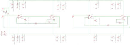
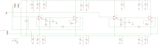
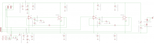
Sergey888 - A first pass at V2.0. 15pF and 1k feedback resistors added. Had to use 0805 size SMD for the feedback parts and the 0.1uF OPA827 bypass caps. I switched decoupling values. The 1.0uF COG MLCC is now across the 4.7uF solid tantalum on the LME49600 rail bypass. The 0.1uF COG MLCCs are on the OPA827 rails. Good point about the X7Rs, for decoupling bigger should beat tempco and voltage stability. I may change those MLCCs to (bigger) X7R.
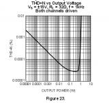
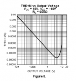
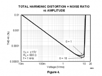
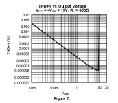
I spent a few hours yesterday studying the THD + noise graphs in the datasheets for the OPA827, LME48720, LME49600 (which the sheet measures looped with the LME49720), the LME49990, and RocketScientist / NwAvGuy's THD + N measurement of the O2 with 6Vrms swing. Interesting stuff. From the datasheets the THD+N at 1kHz with the OPA827 wrapped around the LME49600 should be nearly identical to that with the LME49720. Both about 0.00003% with a 3V swing, 15V rails, 600R load. The LME49600 input impedance will be nowhere near 600 of course, but it just provides some apples-to-apples numbers from the datasheets.
I had to puzzle a while over NwAvGuy's O2 amp THD+N measurements with the 6Vrms swing. Those are just amazingly low THD+N he measurements for the NJM4556A chips in the O2 headphone amp with that large of a voltage swing. The low level of THD+N sure doesn't pop out at me from the little datasheet graph NJM provides in the 4556A datasheet, especially on the 20kHz end of things. I guess the datasheet THD+N measurement being done at 30dB gain is making the difference. At any rate it bodes very well for my ODA amp version with those parallel 4556A's. His posted measurements were verified when Tyll Hertsens re-did them with his Audio Precision tester last year.
THD+N snippets are LME49600 (with LME49720) into 32R, LME49720 into 600R, OPA872 into 600R, LME49990 into 600R. All +/-15Vdc rails and all at 1jHz. At 3Vrms swing the LME49990 is around 0.00001%, the others around 0.00003%. Note the X axis on the LME49600 is watts, so it lets go at 1W = about 5.6Vrms swing. Although the LME49990 has the best THD+N number of the bunch, the OPA827 has the best number that also has gauranteed maximum input offset voltage of just 125uV. The maixmum of the LME49990 is listed as 1000uV. 1000uV = 1mV would still beat the 3mV of the O2 amp, but I would really like to get it down to around 100uV is possible, and do it without using a DC servo. The OPA827 should fit the bill.
15pF and 1k feedback resistors added. Had to use 0805 size SMD for the feedback parts and the 0.1uF OPA827 bypass caps. I switched decoupling values. The 1.0uF COG MLCC is now across the 4.7uF solid tantalum on the LME49600 rail bypass. The 0.1uF COG MLCCs are on the OPA827 rails. Good point about the X7Rs, for decoupling bigger should beat tempco and voltage stability. I may change those MLCCs to (bigger) X7R.I spent a few hours yesterday studying the THD + noise graphs in the datasheets for the OPA827, LME48720, LME49600 (which the sheet measures looped with the LME49720), the LME49990, and RocketScientist / NwAvGuy's THD + N measurement of the O2 with 6Vrms swing. Interesting stuff. From the datasheets the THD+N at 1kHz with the OPA827 wrapped around the LME49600 should be nearly identical to that with the LME49720. Both about 0.00003% with a 3V swing, 15V rails, 600R load. The LME49600 input impedance will be nowhere near 600 of course, but it just provides some apples-to-apples numbers from the datasheets.
I had to puzzle a while over NwAvGuy's O2 amp THD+N measurements with the 6Vrms swing. Those are just amazingly low THD+N he measurements for the NJM4556A chips in the O2 headphone amp with that large of a voltage swing. The low level of THD+N sure doesn't pop out at me from the little datasheet graph NJM provides in the 4556A datasheet, especially on the 20kHz end of things. I guess the datasheet THD+N measurement being done at 30dB gain is making the difference. At any rate it bodes very well for my ODA amp version with those parallel 4556A's. His posted measurements were verified when Tyll Hertsens re-did them with his Audio Precision tester last year.
THD+N snippets are LME49600 (with LME49720) into 32R, LME49720 into 600R, OPA872 into 600R, LME49990 into 600R. All +/-15Vdc rails and all at 1jHz. At 3Vrms swing the LME49990 is around 0.00001%, the others around 0.00003%. Note the X axis on the LME49600 is watts, so it lets go at 1W = about 5.6Vrms swing. Although the LME49990 has the best THD+N number of the bunch, the OPA827 has the best number that also has gauranteed maximum input offset voltage of just 125uV. The maixmum of the LME49990 is listed as 1000uV. 1000uV = 1mV would still beat the 3mV of the O2 amp, but I would really like to get it down to around 100uV is possible, and do it without using a DC servo. The OPA827 should fit the bill.
Attachments
-
 O2 output PCB OPA827 LME49600 circuit.png39 KB · Views: 586
 -
 O2 output PCB OPA827 LME49600 layout lyr 1_4.png137.5 KB · Views: 524
 -
 LME49600_THD+N_vs_power_32R_load.PNG26.1 KB · Views: 565
 -
 LME49720_THD+N_vs_power_600R_load.PNG18.9 KB · Views: 164
 -
 OPA827_THD+N_vs_power_600R_load.PNG21.1 KB · Views: 149
 -
 LME49990_THD+N_vs_power_600R_load.PNG32.5 KB · Views: 142
Last edited:
It fits!
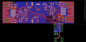
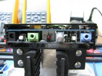
The boards for this project are back already, with one screw-up. The O2 amp case is 100mm wide, not 80mm. What a dumb mistake to make. Depth swapped for width.
But regardless the board answers the DPAK size question. The two LME49600's fit just fine soldered down in the top slot of the O2 headphone amp case. I wasn't expecting that. Even without the board being the full width I can tell both DPAK's will fit by the proximity to the O2 parts underneath. Isn't even a tight fit either, between the DPAKs and the top of the case.
The good news is that extra 20mm of width that I forgot is over the output jack and AC power stuff on the O2 headphone amp, a good place to avoid with the OPA827 input lines.
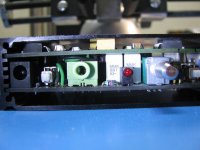
The photos below show:
* the board
* thinly solder coating the PCB DPAK pad and DPAK heat sink with a wide chisel tip on the iron
* Heating the DPAK pad and heatsink while pushing down (yep those are pliers, all grounded and on an anti-stat mat)
* clearance to the case top while inserted in the top slot
* the header that goes in where U3 is on the O2 headphone amp, and a closeup. The wires would be shorter for actual use in the O2, of course, this is just for test since
I botched the PCB width.
* PCB bottom, all the V- rail nail to the top heatsink with the thermal vias. The blank notch sits over the metal endcaps of the O2's two 220uF electrolytic capacitors.
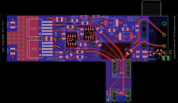
* revised layout and circuit with Sergey888's feedback network and the correct 100mm board width. Even was able to increase the size back to 1206 SMD from 0805.
The boards for this project are back already, with one screw-up. The O2 amp case is 100mm wide, not 80mm.
What a dumb mistake to make. Depth swapped for width. But regardless the board answers the DPAK size question. The two LME49600's fit just fine soldered down in the top slot of the O2 headphone amp case. I wasn't expecting that. Even without the board being the full width I can tell both DPAK's will fit by the proximity to the O2 parts underneath. Isn't even a tight fit either, between the DPAKs and the top of the case.
The good news is that extra 20mm of width that I forgot is over the output jack and AC power stuff on the O2 headphone amp, a good place to avoid with the OPA827 input lines.
The photos below show:
* the board
* thinly solder coating the PCB DPAK pad and DPAK heat sink with a wide chisel tip on the iron
* Heating the DPAK pad and heatsink while pushing down (yep those are pliers, all grounded and on an anti-stat mat)
* clearance to the case top while inserted in the top slot
* the header that goes in where U3 is on the O2 headphone amp, and a closeup. The wires would be shorter for actual use in the O2, of course, this is just for test since
I botched the PCB width.
* PCB bottom, all the V- rail nail to the top heatsink with the thermal vias. The blank notch sits over the metal endcaps of the O2's two 220uF electrolytic capacitors.
* revised layout and circuit with Sergey888's feedback network and the correct 100mm board width. Even was able to increase the size back to 1206 SMD from 0805.
Attachments
-
 IMG_2079.JPG112.4 KB · Views: 239
 -
 IMG_2078.JPG120.6 KB · Views: 268
 -
 IMG_2076.JPG193.3 KB · Views: 231
 -
 IMG_2080.JPG124.2 KB · Views: 225
 -
 IMG_2083.JPG141.8 KB · Views: 234
 -
 IMG_2084.JPG172.1 KB · Views: 264
 -
 IMG_2085.JPG104.8 KB · Views: 240
 -
 IMG_2086.JPG139.2 KB · Views: 211
 -
 O2 output PCB OPA827 LME49600 circuit.png40.2 KB · Views: 206
 -
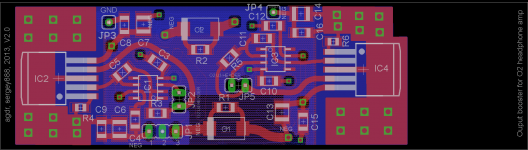 O2 output PCB OPA827 LME49600 layout lyr 1_4.png143 KB · Views: 169
Last edited:
125mW into 8 ohms
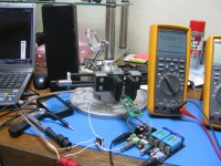
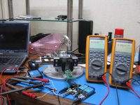
It works. With the OPA140 chip looped around the LME49600 the O2 amp's output DC offset is just 24uV vs. 3.4mV using the O2's standard NJM4556A chip. In a worst-case scenario load test I hooked it up to an 8ohm speaker. The circuit was able to push about 125mW into the speaker. The heatsinking worked better than I expected with the LME49600 get just sligtly warm while dissipating about 1.3W at that point. Can't do that with an NJM4556A chip!
I soldered an OPA140 based loop on one channel of the board and a OPA827 on the other to compare. I had a little accident with the OPA827 end so I don't have those numbers yet. Who knew the brown bar on one end of solid tantalum SMD chips was positive rather than negative?
The photos below are:
* First two show the board still fits just fine in the O2 amp's top slot with the rest of the parts loaded. The 47uF 35V solid tantalum capacitors are about the same height as the LME49600 but they clear the case top with room to spare.
* DC test setup. The input is left unconnected so the jack grounds both channels.
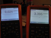
* DC output offset voltage of the OPA140 + LME49600 on the left (24uV) vs. the other channel in the O2 with the NJM4556A chip left installed (3.4mV). A 99.3% reduction!
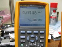
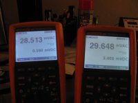
* Next 2 photos are an AC test with music going in. I'm using fairly sensitive 114dB/V headphones here, so the 28mV (rms) shown represents normal listening levels and 64mV(rms) very loud levels. Still just 190uV instantaneous DC output offset voltage on the OPA140+LME49600 channel vs. 3.4mV on the NJM4556A channel.
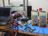
* Next 3 photos are a speaker test setup! My test headphones present a rediculously low load at 28mV(rms), so I wanted to try a load that would push the LME49600 to the limit. That black tower speaker is an 8ohm unit. I didn't whip out the scope, but I could hear distortion starting at about 1.3Vrms. 1Vrms into 8ohms would be 125mW and a current of 1/8 = 125mA (rms). That leaves 11V across the LME49600 with the O2's +/-12V power rails, so it dissipates 11 * .125mA = 1.37W. Only got slightly warm at that level. I'm impressed at how well the thermal vias are working. Only 16mV of DC offset into the speaker at 1.01Vac (rms).
It works.
With the OPA140 chip looped around the LME49600 the O2 amp's output DC offset is just 24uV vs. 3.4mV using the O2's standard NJM4556A chip. In a worst-case scenario load test I hooked it up to an 8ohm speaker. The circuit was able to push about 125mW into the speaker. The heatsinking worked better than I expected with the LME49600 get just sligtly warm while dissipating about 1.3W at that point. Can't do that with an NJM4556A chip! I soldered an OPA140 based loop on one channel of the board and a OPA827 on the other to compare. I had a little accident with the OPA827 end so I don't have those numbers yet. Who knew the brown bar on one end of solid tantalum SMD chips was positive rather than negative?
The photos below are:
* First two show the board still fits just fine in the O2 amp's top slot with the rest of the parts loaded. The 47uF 35V solid tantalum capacitors are about the same height as the LME49600 but they clear the case top with room to spare.
* DC test setup. The input is left unconnected so the jack grounds both channels.
* DC output offset voltage of the OPA140 + LME49600 on the left (24uV) vs. the other channel in the O2 with the NJM4556A chip left installed (3.4mV). A 99.3% reduction!
* Next 2 photos are an AC test with music going in. I'm using fairly sensitive 114dB/V headphones here, so the 28mV (rms) shown represents normal listening levels and 64mV(rms) very loud levels. Still just 190uV instantaneous DC output offset voltage on the OPA140+LME49600 channel vs. 3.4mV on the NJM4556A channel.
* Next 3 photos are a speaker test setup! My test headphones present a rediculously low load at 28mV(rms), so I wanted to try a load that would push the LME49600 to the limit. That black tower speaker is an 8ohm unit. I didn't whip out the scope, but I could hear distortion starting at about 1.3Vrms. 1Vrms into 8ohms would be 125mW and a current of 1/8 = 125mA (rms). That leaves 11V across the LME49600 with the O2's +/-12V power rails, so it dissipates 11 * .125mA = 1.37W. Only got slightly warm at that level. I'm impressed at how well the thermal vias are working. Only 16mV of DC offset into the speaker at 1.01Vac (rms).
Attachments
-
 IMG_2088.JPG151.3 KB · Views: 208
 -
 IMG_2091.JPG214.8 KB · Views: 251
 -
 IMG_2093.JPG205.3 KB · Views: 236
 -
 IMG_2096.JPG115.9 KB · Views: 196
 -
 IMG_2101.JPG155.7 KB · Views: 173
 -
 IMG_2106.JPG115.1 KB · Views: 174
 -
 IMG_2099.JPG204.6 KB · Views: 164
 -
 IMG_2098.JPG114.7 KB · Views: 169
 -
 IMG_2097.JPG202.6 KB · Views: 172
Last edited:
OPA140 DC offset lower than OPA827
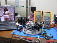
I was able to get the OPA827+LME49600 end of this project board going with a surprising result: the DC offset of the OPA140+LME49600 is a lot lower than the more expensive OPA827. Both sound terrific though, subjectively.
The photos below:
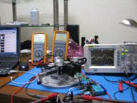
* The first two photos are the test setup, running on batteries this time rather than the AC adapter. The inputs are grounded. The O2 amp's other NJM4556A chip is gone, with a header running the wires to the OPA827 section. The meter on the left is the OPA827+LME49600 end of the board. The meter on the right is the OPA140+LME49600 end. 24uV for the OPA827 loop, just 1uV for the OPA140 loop. lol - the OPA140's DC was so close to zero that I had to keep occationally injecting noise with my finger to verify a test lead hadn't popped off somewhere.
* closeup of the displays a minute later. The OPA827 loop had wandered a bit to 29uV.
* AC test with music playing and sensitive headphones. Instantaneous values of around 22mVac (rms) on both channels, about mid-volume for the test headphones, with 143uV of DC offset for the OPA827 loop and 15mV for the OPA140 loop.
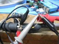
* Stability and oscillation test setup with an axial 1000pf MLCC capacitor placed across each headphone output, with the headphones connected.
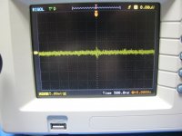
* scope shot of the OPA140 loop channel with amplifier inputs grounded. No signs of oscillation at all, at least to the 5mV/div limit of the scope. Combined probe + scope bandwidth is probably around 80mHz at the 3dB point, so it could miss any higher frequency oscillation. Both OPAs and both LME49600s are running cool though, so most likely no higher oscillation occuring.
* for comparison, a scope shot with the O2 amp turned off (just random background noise).
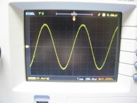
* scope shot of a 1kHz signal playing through the O2.
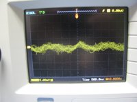
* scope shot with music playing.
The scope shots of the OPA827 loop channel were similar. No signs of oscillation. Sergey888's feedback loop is still a really good idea though. I'll add it to the next version. Certainly can't hurt.
And... a typo on my previous post. The DC offset with the 1Vac (rms) into the 8 ohm speaker is 1.6mV, as can be seen in the photo, not 16mV.
I was able to get the OPA827+LME49600 end of this project board going with a surprising result: the DC offset of the OPA140+LME49600 is a lot lower than the more expensive OPA827. Both sound terrific though, subjectively.
The photos below:
* The first two photos are the test setup, running on batteries this time rather than the AC adapter. The inputs are grounded. The O2 amp's other NJM4556A chip is gone, with a header running the wires to the OPA827 section. The meter on the left is the OPA827+LME49600 end of the board. The meter on the right is the OPA140+LME49600 end. 24uV for the OPA827 loop, just 1uV for the OPA140 loop. lol - the OPA140's DC was so close to zero that I had to keep occationally injecting noise with my finger to verify a test lead hadn't popped off somewhere.
* closeup of the displays a minute later. The OPA827 loop had wandered a bit to 29uV.
* AC test with music playing and sensitive headphones. Instantaneous values of around 22mVac (rms) on both channels, about mid-volume for the test headphones, with 143uV of DC offset for the OPA827 loop and 15mV for the OPA140 loop.
* Stability and oscillation test setup with an axial 1000pf MLCC capacitor placed across each headphone output, with the headphones connected.
* scope shot of the OPA140 loop channel with amplifier inputs grounded. No signs of oscillation at all, at least to the 5mV/div limit of the scope. Combined probe + scope bandwidth is probably around 80mHz at the 3dB point, so it could miss any higher frequency oscillation. Both OPAs and both LME49600s are running cool though, so most likely no higher oscillation occuring.
* for comparison, a scope shot with the O2 amp turned off (just random background noise).
* scope shot of a 1kHz signal playing through the O2.
* scope shot with music playing.
The scope shots of the OPA827 loop channel were similar. No signs of oscillation. Sergey888's feedback loop is still a really good idea though. I'll add it to the next version. Certainly can't hurt.
And... a typo on my previous post. The DC offset with the 1Vac (rms) into the 8 ohm speaker is 1.6mV, as can be seen in the photo, not 16mV.
Attachments
-
 IMG_2112.JPG205.6 KB · Views: 581
 -
 IMG_2113.JPG187.8 KB · Views: 569
 -
 IMG_2114.JPG71.9 KB · Views: 568
 -
 IMG_2119.JPG63.7 KB · Views: 534
 -
 IMG_2124.JPG136.2 KB · Views: 142
 -
 IMG_2123.JPG129.7 KB · Views: 150
 -
 IMG_2122.JPG143.9 KB · Views: 168
 -
 IMG_2121.JPG172.6 KB · Views: 538
 -
 IMG_2127.JPG196 KB · Views: 175
Last edited:
Sergey888 - it actually did smoke on first power-up. I had the tantalums, C13 and C14, in backwards. C13 lasted about 3 seconds then went up in smoke. I doubled checked voltage and polarity - all OK - and replaced it with a second one. That went up in smoke too. I'm new to the SMD stuff. Why on earth would they put a band on the positive end of a part? Lol. Luckily I forgot to order the 47uF tantalums in my first order from Mouser, or they would have gone up in smoke too.
Hey good find with those OPA140's! I think that is the "standard" op amp for this project. Low quiescent current, low DC offset, low cost, and sounds great.
I have to use the 5cm x 10cm standard fab size from Seeed studio for the 28mm x 100mm board. I just realized the board doesn't have to be rectangular. I could extend a tab right over the O2 amp's NJM4556's to reduce the amount of wiring going to the dip headers and still stay within 5cm x 100cm. I was even considering using solid pins between the boards, but too great a chance of a registration error in lining them up. The wiring allows for some flex.
I had the tantalums, C13 and C14, in backwards. C13 lasted about 3 seconds then went up in smoke. I doubled checked voltage and polarity - all OK - and replaced it with a second one. That went up in smoke too. I'm new to the SMD stuff. Why on earth would they put a band on the positive end of a part? Lol. Luckily I forgot to order the 47uF tantalums in my first order from Mouser, or they would have gone up in smoke too.Hey good find with those OPA140's! I think that is the "standard" op amp for this project. Low quiescent current, low DC offset, low cost, and sounds great.
I have to use the 5cm x 10cm standard fab size from Seeed studio for the 28mm x 100mm board. I just realized the board doesn't have to be rectangular. I could extend a tab right over the O2 amp's NJM4556's to reduce the amount of wiring going to the dip headers and still stay within 5cm x 100cm. I was even considering using solid pins between the boards, but too great a chance of a registration error in lining them up. The wiring allows for some flex.
Attachments
Last edited:
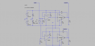
Sergey888 - it looks like I'm going to have room for your second order feedback loops after all. Does this circuit look like what you had in mind? Two 33pF in series with the 3.3K to ground, and the 1K back from the LME49600 output.
I think that I am going to try solid DIP headers after all to eliminate a pile of connecting wires. The board will have the tab with 12 pins that just plugs right into the U3 socket and the top 4 pins of U4 on the O2 amp board. The change makes this truely a "plug-in" upgrade to NwAvGuy's O2 amp. Those are not chips out on the tab. I just created a modified DIP8 socket part in the Eagle library. A 4 pin straight header would actually solder in each side, like #649-68024-413HLF at Mouser, with 4 in a row snapped off for U3 and 3 snapped off for the top 3 pins of U3 (two on board an one with the connecting wire).
That connects everything but ground and one OPA140 input, which will be the only remaining connections needing wires. That input is extended out to the tab, though, so it is just a few millimeters from pin 3 on U4 where it goes with a single pin header. I ran out of board area there with the 5cm fab restriction (staying within the 10cm x 5cm size at Seeed Studio for 4 layer), otherwise the whole U4 header could have been out on the tab too.
I've added another 47uF tantalum rail-to-rail in addition to the two going rail-to-ground.
The tab will mean the board couldn't be panelized 3 to a 10cm x 10 cm fab area, but still could get two in.
I think that I am going to try solid DIP headers after all to eliminate a pile of connecting wires.
The board will have the tab with 12 pins that just plugs right into the U3 socket and the top 4 pins of U4 on the O2 amp board. The change makes this truely a "plug-in" upgrade to NwAvGuy's O2 amp. Those are not chips out on the tab. I just created a modified DIP8 socket part in the Eagle library. A 4 pin straight header would actually solder in each side, like #649-68024-413HLF at Mouser, with 4 in a row snapped off for U3 and 3 snapped off for the top 3 pins of U3 (two on board an one with the connecting wire).That connects everything but ground and one OPA140 input, which will be the only remaining connections needing wires. That input is extended out to the tab, though, so it is just a few millimeters from pin 3 on U4 where it goes with a single pin header. I ran out of board area there with the 5cm fab restriction (staying within the 10cm x 5cm size at Seeed Studio for 4 layer), otherwise the whole U4 header could have been out on the tab too.
I've added another 47uF tantalum rail-to-rail in addition to the two going rail-to-ground.
The tab will mean the board couldn't be panelized 3 to a 10cm x 10 cm fab area, but still could get two in.
Attachments
Last edited:
agdr
Yep, it looks correct.
Beside, in this particular case with unity gain you can connect 3.3k resistor to output of LME with very similar result.
Can I ask you what is the purpose of R1 R2?
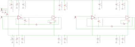
I still think having two LME on different sides of PCB is not ideal solution. It can be a bit awkward mechanically, but I would place them side by side, and use dual OPA2140. Dual opaamp pinout is actually more layout friendly.
Yep, it looks correct.
Beside, in this particular case with unity gain you can connect 3.3k resistor to output of LME with very similar result.
Can I ask you what is the purpose of R1 R2?
I still think having two LME on different sides of PCB is not ideal solution. It can be a bit awkward mechanically, but I would place them side by side, and use dual OPA2140. Dual opaamp pinout is actually more layout friendly.
Sergey888 - R1 and R2 are a modification for the O2 headamp that I figured I would add to this board since I had some space left over. They help prevent turn-off thumps. NwAvGuy only had chips as the load on the power rails after the power management mosfets. The resistors help with a linear drain to zero volts below the chips' minimum power supply voltages. So R1 and R2 are optional.
Good thoughts about putting the LME49600s side by side! That actually hadn't occured to me all. I guess that I was focused on maximum heat dissipation by putting them on the ends of the board. The thermal vias work a lot better than I thought they would.
I just whipped up a quick version with the side-by-side LNE49600s and the OPA2140. That does reduce the parts count quite a bit. It looks like DIY Audio's picture upload function is broken right now, so I have the layout, schematic, and BOM here on Google Drive:
https://drive.google.com/folderview?id=0B67cJELZW-i8MFBoS3c1REpNN1U&usp=sharing
I've updated the BOM with the 10uF X7R MLCC's replacing the 4.7uF tantalums for decoupling on the LME49600's. No need for the 0.1uF bypassing MLCCs anymore on those, just on the OPA2140. That rectangular gap in the bottom metal is where the board sits right over two of the O2's electrolytic caps with metal tops. I'm leaving pads for the LME49600's bandwidth resistor pads out entirely. There is just no earthly need I'm aware of to use 180mHz bandwidth for audio, with the associated double quiescent current draw and high(er) frequency oscillation potential.
I'm down to only one connecting wire now, just ground! I realized last night that since the board now plugs into the O2's U3 and U4 dip sockets it won't rattle around and doesn't exactly need to be flush with the front panel anymore. I had it wedged between the front panel and battery connectors, in the top case slot. I moved it 2mm back from the front panel, which added 2mm to the end of the tab (staying within the 5cm fab limit), enough to add a 3rd row of pins on U4 and connect that input.
Good thoughts about putting the LME49600s side by side! That actually hadn't occured to me all. I guess that I was focused on maximum heat dissipation by putting them on the ends of the board. The thermal vias work a lot better than I thought they would.
I just whipped up a quick version with the side-by-side LNE49600s and the OPA2140. That does reduce the parts count quite a bit. It looks like DIY Audio's picture upload function is broken right now, so I have the layout, schematic, and BOM here on Google Drive:
https://drive.google.com/folderview?id=0B67cJELZW-i8MFBoS3c1REpNN1U&usp=sharing
I've updated the BOM with the 10uF X7R MLCC's replacing the 4.7uF tantalums for decoupling on the LME49600's. No need for the 0.1uF bypassing MLCCs anymore on those, just on the OPA2140. That rectangular gap in the bottom metal is where the board sits right over two of the O2's electrolytic caps with metal tops. I'm leaving pads for the LME49600's bandwidth resistor pads out entirely. There is just no earthly need I'm aware of to use 180mHz bandwidth for audio, with the associated double quiescent current draw and high(er) frequency oscillation potential.
I'm down to only one connecting wire now, just ground!
I realized last night that since the board now plugs into the O2's U3 and U4 dip sockets it won't rattle around and doesn't exactly need to be flush with the front panel anymore. I had it wedged between the front panel and battery connectors, in the top case slot. I moved it 2mm back from the front panel, which added 2mm to the end of the tab (staying within the 5cm fab limit), enough to add a 3rd row of pins on U4 and connect that input.
Last edited:
I'm adding "upgrade board" for the O2 headphone amp to this thread title since I've also added a few modifications to the O2 that I previously posted in the O2 modification thread. I had some extra board space so might as well.
The board now optionally includes:
The files are also on Google Drive at:
https://drive.google.com/folderview?id=0B67cJELZW-i8S0ZnMm1RWmlKc28&usp=sharing
Once the PC board is back from fabrication and tested I'll post the Gerber files out at that link.
The board now optionally includes:
- After-mosfet power LEDs on each rail. The O2's let says when the power switch is on but says nothing about whether the mosfets have switch (power management circuit) and if both power rails are up. The LEDs are in series with the anti-thump turn-off resistors so just make use of that existing current flow.
- Anti-turn-off-thump resistors to bleed the post-mosfet power rails linearly to ground.
- Power management circuit latch circuit. Prevents the O2 from "motorboating" or "oscillating" when the batteries run down, due to the batteries recharging a bit when the mosfets cut off. Requires two additional wires from the new board to the O2 board. Optional to populate.
- 1/4" neutrik output jack. If the taller B3-080 case is used there is enough space above the O2' 1/8" output jack and on/off switch to mount a 1/4" slimline Neutrik jack upside down on the bottom of the new board. The board hooks it into the new outputs automatically, so it is plug-and-play ready to go. Adding 1/4" jacks to the O2 using the B3-080 case have seemed to be a popular modification.
The files are also on Google Drive at:
https://drive.google.com/folderview?id=0B67cJELZW-i8S0ZnMm1RWmlKc28&usp=sharing
Once the PC board is back from fabrication and tested I'll post the Gerber files out at that link.
Attachments
Last edited:
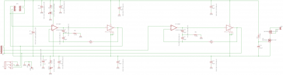
Sergey888 - while updating the build instructions I remembered why I was hanging onto the single op-amp layout, so that the board could also optionally be used with OPA827, OPA627, OPA1641, LME49710 and LME49990 chips along with the OPA140. So even though it is more space-inefficient I've gone back to two single OPA140s instead of the one dual OPA2140. I've kept the two LME49600s side by side though. Thanks again for all the design input! I've made note of that in the updated build instructions and on the board.
Some other things I've tinkered with:
* The decoupling caps on the OPA140 chips are now the same 2.2uF 50V X7Rs MLCC used in the power management latch circuit, up from 0.1uF COG previously - another good suggestion from Sergey888.
* The signal lines feeding the upside down 1/4" jack now have zero ohm resistors in series to disconnect the jack from the LME49600's on the O2 upgrade board. Allows the jack to use used independently from the rest of the board, and/or the board used just for the jack (wired into the O2's P2 connector instead).
* All the layers directly under the two op amps are cut out, helping to prevent any input to output stray capacitance.
* All the V+ power and output signal traces are "doubled nailed" with two vias to lower via impedance and increase current handling ability.
* The LME49600 output lines now go to both O2 NJM4556A socket "paralleled" output pins on U3 and U4 to run the signal through both of the O2's 1R resistors on each channel, keeping the output impedance at 0.5R. The resistors are really not needed through with the LME49600, of course. One of the O2's 1R resistors on each channel can simply be shorted across under the board to get nearly zero output impedance. But this way the board remains plug and play without having to do that.
Here is a Google Drive link to all the versions of the board. The folder with the latest date is the latest version.
https://drive.google.com/folderview?id=0B67cJELZW-i8Vmp5MDVLNzJxTGc&usp=sharing
The Google Drive link also has PDF versions of the circuit layout that can be blown up as big as needed, plus it has png's of each layer individually.
The BOM and build instructions now include all the O2 modification sections, plus how to (optionally) upgrade the O2's power rail voltage to +/-15Vdc after the O2 upgrade board is completed.
Attachments
Last edited:
It fits and it works!
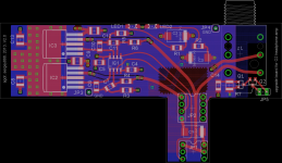
The PC boards for this project arrived today. I just built one up and much to my surprise it not only fits mechanically in the O2, but it works! Didn't screw anything up.
If all goes well with some additional testing I'll post the PC board Gerbers at the Google Drive link above and will sell off the extras in the vendor thread at cost.
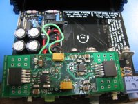
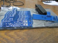
The first photo below is the boards being CAT scanned.
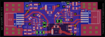
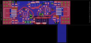
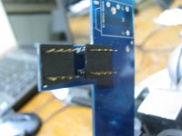
The next two photos show the front and back of the PC board. This is one of the stranger shaped PC boards out there. I went with a blue solder mask this time for something different.
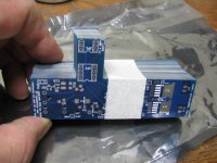
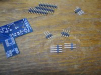
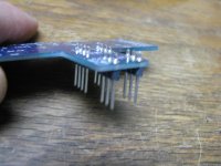
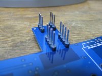
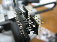
The next 3 photos show one of the linear SIP headers being snipped with wire cutters into two 4 pin sections and two 3 pin sections. Those are then inserted into the bottom of the PCB board in the two IC holes in the tab and soldered (on the top of the PC board). They don't have to be exactly straight since they are going to be bent in the next step anyway, but I used a second one of the PC boards slipped over the free ends to align them while soldering.
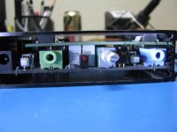
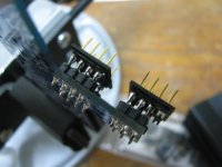
The next 3 photos show those SIP pins being cut to 2.4mm long with wire cutters, bent outward slightly so they fit on the outside of the coined contacts on the DIP8 headers, then soldered to the header contacts. The net result is the two 8 pin DIP headers ready to plug into the O2 amp's U3 and U4 socket.
I wanted to build up this header contact portion first to make sure I hadn't screwed up the mechanical measurements. The final photo shows the header contacts plugged into the O2 and the whole thing slid into the B2-080 case bottom (O2 PCB) and top (O2 boost board) slots. It fits!
I'm out of picture posting slots on this post, so part 2 will be posted next...
The PC boards for this project arrived today. I just built one up and much to my surprise it not only fits mechanically in the O2, but it works! Didn't screw anything up.
If all goes well with some additional testing I'll post the PC board Gerbers at the Google Drive link above and will sell off the extras in the vendor thread at cost.
The first photo below is the boards being CAT scanned.
The next two photos show the front and back of the PC board. This is one of the stranger shaped PC boards out there. I went with a blue solder mask this time for something different.
The next 3 photos show one of the linear SIP headers being snipped with wire cutters into two 4 pin sections and two 3 pin sections. Those are then inserted into the bottom of the PCB board in the two IC holes in the tab and soldered (on the top of the PC board). They don't have to be exactly straight since they are going to be bent in the next step anyway, but I used a second one of the PC boards slipped over the free ends to align them while soldering.
The next 3 photos show those SIP pins being cut to 2.4mm long with wire cutters, bent outward slightly so they fit on the outside of the coined contacts on the DIP8 headers, then soldered to the header contacts. The net result is the two 8 pin DIP headers ready to plug into the O2 amp's U3 and U4 socket.
I wanted to build up this header contact portion first to make sure I hadn't screwed up the mechanical measurements. The final photo shows the header contacts plugged into the O2 and the whole thing slid into the B2-080 case bottom (O2 PCB) and top (O2 boost board) slots. It fits!
I'm out of picture posting slots on this post, so part 2 will be posted next...
Attachments
-
 IMG_2155.JPG204.7 KB · Views: 205
 -
 IMG_2152.JPG155.7 KB · Views: 198
 -
 IMG_2151.JPG227.4 KB · Views: 177
 -
 IMG_2156.JPG210.4 KB · Views: 179
 -
 IMG_2159.JPG141.4 KB · Views: 172
 -
 IMG_2161.JPG133 KB · Views: 181
 -
 IMG_2162.JPG122.2 KB · Views: 167
 -
 IMG_2163.JPG127.6 KB · Views: 164
 -
 IMG_2166.JPG112.8 KB · Views: 154
 -
 IMG_2172.JPG118.9 KB · Views: 182
Last edited:
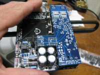
Build and test photos, part 2...
The first three photos are more shots of the O2 booster PCB mated with the O2 PCB, since I ran out of picture posting slots above.
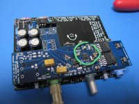
Next photo shows soldering on the LM49600s with a wide tip on the iron.
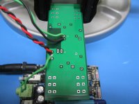
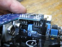
The mext photo is all the amp parts soldered on. I haven't soldered on any of the O2 modification parts yet, just wanted to test the amp at this point. There is no real order to soldering on the rest of the parts, with two exceptions.
The first is that I did manage to fit in pads for the LME49600 bandwith resistors R7 and R10. Normally these are left unconnected (no resistors soldered on) since the 110mHz "low" bandwidth is more than enough for audio and is the low(er) 7mA idle current mode. But if someone really wants to put it in high bandwidth mode, there are the pads. If those two resistors are used they should be soldered on before the LME49600s given how close they are to the chip, although I believe I could have still soldered them on after if needed.
Then the other soldering-order thing is to leave the two OPA140s (or OPA827s, whatever you are using) for last given the static sensitive jfet input pins. There is no resistor to ground on the jfet inputs on the board since it relies on the O2's 40.2K resistors to ground once plugged into the O2. Best to get the rest of the passive parts on there first. There is plenty of room for drag soldering those two chips even after all the other SMD parts are on. Then double check (triple check!) all the solder connections with a magnifying glass for bridges or opens. Note that I'm using an anti-static mat at this point with the iron grounded and a grounded wrist strap.
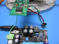
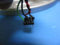
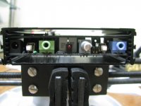
The green wire is the ground going from JP3 ground hole to the nearby ground of the batteries (middle two batt connectors). The wire doen't have to be nearly that long, of course, I just quickly cut a section of wire and soldered it on to get the measurement show on the road. Another good ground to use is a wire under the board from the JP4 ground hole up front to the ground hole in the O2's P2 jack. You only have to use one or the other ground - your choice - but don't use both. This one ground wire is the only part of the amp that doesn't go through the DIP headers.
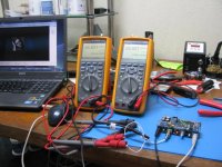
The next photo shows the DC test setup since I want to measure output DC offset on both channels first. Two DMMs and some test headphones plugged in.
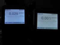
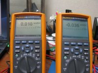
The next photo shows the O2 amp's new DC offset with the boost board: 10uV and 36uV on the two channels! That is MICRO volts, a 98%+ reduction over the O2's usual 3mV = 3000uV DC offset with the NJM4556A chips.
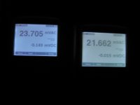
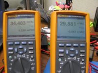
The next photo shows instantaneous AC and DC captures with music playing. Very sensitive headphones being used, so the 30mV (rms) represents normal listening levels. The instantaneous DC offsets on the two channels read 124uV and 47uV. Instantaneous DC offset jumps around a little bit with the music, of course, since the music's instantateous DC level fluctuates.
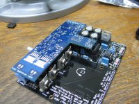
The final photo shows fit of the board with all the amp components soldered on, especially the LME49600s and the two 47uF tantalum capacitors which are the tallest. Fits perfectly. I had to pull the metal top of the B2 case up just very slightly to clear the LME49600s to compensate for it not being flat to start with (slight downward bend).
And... quite subjectively, it sounds great! These sensitive headphones are useless for significantly loading the LME49600s. I'm going to attach it to 8 ohm desk speakers again for an abuse test and see how it fares, along with using some less sensitive headphones.
Thanks again to Sergey888 for the great suggestions of the OPA140, the side-by-side LM49600s, and that 2nd order feedback loop! I'm going to throw it on the scope to check for osciallation, but at this point the chips are completely cool. No thermal signs anyway of bad stuff happening.
The first three photos are more shots of the O2 booster PCB mated with the O2 PCB, since I ran out of picture posting slots above.
Next photo shows soldering on the LM49600s with a wide tip on the iron.
The mext photo is all the amp parts soldered on. I haven't soldered on any of the O2 modification parts yet, just wanted to test the amp at this point. There is no real order to soldering on the rest of the parts, with two exceptions.
The first is that I did manage to fit in pads for the LME49600 bandwith resistors R7 and R10. Normally these are left unconnected (no resistors soldered on) since the 110mHz "low" bandwidth is more than enough for audio and is the low(er) 7mA idle current mode. But if someone really wants to put it in high bandwidth mode, there are the pads. If those two resistors are used they should be soldered on before the LME49600s given how close they are to the chip, although I believe I could have still soldered them on after if needed.
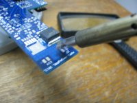
Then the other soldering-order thing is to leave the two OPA140s (or OPA827s, whatever you are using) for last given the static sensitive jfet input pins. There is no resistor to ground on the jfet inputs on the board since it relies on the O2's 40.2K resistors to ground once plugged into the O2. Best to get the rest of the passive parts on there first. There is plenty of room for drag soldering those two chips even after all the other SMD parts are on. Then double check (triple check!) all the solder connections with a magnifying glass for bridges or opens. Note that I'm using an anti-static mat at this point with the iron grounded and a grounded wrist strap.
The green wire is the ground going from JP3 ground hole to the nearby ground of the batteries (middle two batt connectors). The wire doen't have to be nearly that long, of course, I just quickly cut a section of wire and soldered it on to get the measurement show on the road. Another good ground to use is a wire under the board from the JP4 ground hole up front to the ground hole in the O2's P2 jack. You only have to use one or the other ground - your choice - but don't use both. This one ground wire is the only part of the amp that doesn't go through the DIP headers.
The next photo shows the DC test setup since I want to measure output DC offset on both channels first. Two DMMs and some test headphones plugged in.
The next photo shows the O2 amp's new DC offset with the boost board: 10uV and 36uV on the two channels!
That is MICRO volts, a 98%+ reduction over the O2's usual 3mV = 3000uV DC offset with the NJM4556A chips. The next photo shows instantaneous AC and DC captures with music playing. Very sensitive headphones being used, so the 30mV (rms) represents normal listening levels. The instantaneous DC offsets on the two channels read 124uV and 47uV. Instantaneous DC offset jumps around a little bit with the music, of course, since the music's instantateous DC level fluctuates.
The final photo shows fit of the board with all the amp components soldered on, especially the LME49600s and the two 47uF tantalum capacitors which are the tallest. Fits perfectly. I had to pull the metal top of the B2 case up just very slightly to clear the LME49600s to compensate for it not being flat to start with (slight downward bend).
And... quite subjectively, it sounds great!
These sensitive headphones are useless for significantly loading the LME49600s. I'm going to attach it to 8 ohm desk speakers again for an abuse test and see how it fares, along with using some less sensitive headphones.Thanks again to Sergey888 for the great suggestions of the OPA140, the side-by-side LM49600s, and that 2nd order feedback loop! I'm going to throw it on the scope to check for osciallation, but at this point the chips are completely cool. No thermal signs anyway of bad stuff happening.
Attachments
-
 IMG_2176.JPG190.2 KB · Views: 178
 -
 IMG_2169.JPG161.1 KB · Views: 205
 -
 IMG_2168.JPG234.1 KB · Views: 224
 -
 IMG_2177.JPG145.2 KB · Views: 177
 -
 IMG_2178.JPG182.3 KB · Views: 219
 -
 IMG_2182.JPG203.2 KB · Views: 201
 -
 IMG_2187.JPG166.4 KB · Views: 140
 -
 IMG_2184.JPG162.2 KB · Views: 136
 -
 IMG_2189.JPG147.9 KB · Views: 177
Last edited:
- Home
- Amplifiers
- Headphone Systems
- O2 headamp output booster PCB