Hey all,
I've made a few CMOYs on perfboard, and played around with some power schemes. Wanted to make a PCB, and then decided to add in crossfeed, and power, and then wondered if I could get it all on the same board, and make it as flexible as possible for experimenting,
and make it fit ExpressPCBs 3.8 x 2.5 footprint (cheapest option). Well, this is it.
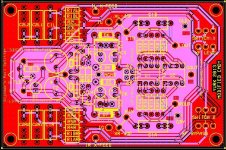
Completely loaded, it uses Sijosae's rail splitter, Tangent's modified Linkwitz crossfeed (HI-Z version), and Apheared's 47 CMOY.
All the power grounds are on the bottom ground plane, and the signal grounds are on the top ground plane. All these get tied together at Main ground (MGND). I tried to get all the traces on the bottom of the board that I possibly could.
Options:
All resistors in the crossfeed and the cmoy circuit are spaced 0.1 inches for SIP rails, if you'd like even more flexibility. Left room for OPAMP sockets.
Power:
You can use Sijosae's rail splitter to feed the regulators, or use a TLE. If you don't want the regulators on the board, you can bypass them. If you have a split supply already, you can bypass all the power circuitry on the board and use that. All of that's spelled out in the schematic as to which connections and parts need to be used/jumpered/omitted. Also added space for small bypass caps by the OPAMPS.
Crossfeed:
You can use it or not. Different inputs for not using it, need jumpers if you do use it. Again, that's in the schematic too. Layout can use caps with lead spacing from 0.2, 0.3, 0.4, 0.5, 0.6 inches, so everyone should be able to fit (most of) their favorite film caps.
CMOY:
This is pretty much Apheared's 47 CMOY, don't think I changed anything schematic wise, just a different board layout. Caps use same footprint as the ones in the crossfeed section.
Biggest problem is that there isn't any room on the board for jacks. Everything has to be done with flywires.
If you wanted to attach this board to something, the mounting holes should accomodate #4 machine bolts.
So, this is my crazy layout I'm going to be experimenting with, what stands out as the worst thing(s) about it? See something I missed? Just want to comment about how crazy I am? All comments welcome.
Yurk
I've made a few CMOYs on perfboard, and played around with some power schemes. Wanted to make a PCB, and then decided to add in crossfeed, and power, and then wondered if I could get it all on the same board, and make it as flexible as possible for experimenting,
and make it fit ExpressPCBs 3.8 x 2.5 footprint (cheapest option). Well, this is it.
Completely loaded, it uses Sijosae's rail splitter, Tangent's modified Linkwitz crossfeed (HI-Z version), and Apheared's 47 CMOY.
All the power grounds are on the bottom ground plane, and the signal grounds are on the top ground plane. All these get tied together at Main ground (MGND). I tried to get all the traces on the bottom of the board that I possibly could.
Options:
All resistors in the crossfeed and the cmoy circuit are spaced 0.1 inches for SIP rails, if you'd like even more flexibility. Left room for OPAMP sockets.
Power:
You can use Sijosae's rail splitter to feed the regulators, or use a TLE. If you don't want the regulators on the board, you can bypass them. If you have a split supply already, you can bypass all the power circuitry on the board and use that. All of that's spelled out in the schematic as to which connections and parts need to be used/jumpered/omitted. Also added space for small bypass caps by the OPAMPS.
Crossfeed:
You can use it or not. Different inputs for not using it, need jumpers if you do use it. Again, that's in the schematic too. Layout can use caps with lead spacing from 0.2, 0.3, 0.4, 0.5, 0.6 inches, so everyone should be able to fit (most of) their favorite film caps.
CMOY:
This is pretty much Apheared's 47 CMOY, don't think I changed anything schematic wise, just a different board layout. Caps use same footprint as the ones in the crossfeed section.
Biggest problem is that there isn't any room on the board for jacks. Everything has to be done with flywires.
If you wanted to attach this board to something, the mounting holes should accomodate #4 machine bolts.
So, this is my crazy layout I'm going to be experimenting with, what stands out as the worst thing(s) about it? See something I missed? Just want to comment about how crazy I am? All comments welcome.
Yurk
Attachments
True, EpressPCB would cost about twice as much as 3 boards from OSHpark. And those OSHpark boards look awesome!
Unfortunately, I absolutely HATE Eagle. I did a few designs with it, spent several weeks with it, and kept waiting for that ahaa moment that everyone seems to have -- use Eagle long enough, and you'll like it. Didn't happen for me.
Have heard some good things about Kicad, may give it a try.
Noticed last night that my MGND that is supposed to tie both top and bottom planes together (GND and AGND) isn't connected to the top plane, just the bottom. Guess I'll have to add a another hole that's tied to the top plane and jumper them together? Anybody have a way for a hole to join two different nets and pass DRC/ERC?
Thanks, I just tried that. Didn't quite do what I wanted though. By renaming one plane to GND to match the other plane, it disconnected everything that was attached to AGND.
I've got all the power supply gnds on one plane, and the signal ground on the other plane, and I want them to join at only one point (even though it's a floating ground, not a real ground, etc).
In ExpressPCB, I just told it to put thermals on top and bottom of hole MGND, and it was happy. Eagle is trying to protect me from myself, and won't let me do what I want. Very frustrating.
OK, I got it working.
I just changed the name of the top polygon
the GND.
Just give all of your grounds the same name.
The copper and electrons don't care what you
call them. If it needs to connect, give it the
same name.
By the way, what you built is an Apheared 47, not a CMoy.
Cheers and happy building.
I just changed the name of the top polygon
the GND.
Just give all of your grounds the same name.
The copper and electrons don't care what you
call them. If it needs to connect, give it the
same name.
By the way, what you built is an Apheared 47, not a CMoy.
Cheers and happy building.
Last edited:
Thanks for your all your help. Naming all the grounds the same will connect them, but I wanted to keep certain grounds on the top of the board, and certain ones on the bottom of the board. I realize it's not necessary in this simple circuit, but I wanted to try it anyway. ")
So, I'll just add another hole that's tied to AGND and jumper it to MGND. It's not as elegant as what I wanted (one hole), but it will serve the purpose. This is something I'll have to keep digging at before I get into more complicated designs. Or, the two hole method may be the easiest way. (In Eagle). I realize this is a special purpose sort of thing, not really needed, as most keep all their grounds on the same plane.
Oh, and I should've changed the title to Apheared 47, I think I did mention it somewhere in the first post. I haven't added all my comments to the Eagle schematics to explain a lot of the options on the board either.
Thanks again Avro for all your help and time in answering my stupid questions!
So, I'll just add another hole that's tied to AGND and jumper it to MGND. It's not as elegant as what I wanted (one hole), but it will serve the purpose. This is something I'll have to keep digging at before I get into more complicated designs. Or, the two hole method may be the easiest way. (In Eagle). I realize this is a special purpose sort of thing, not really needed, as most keep all their grounds on the same plane.
Oh, and I should've changed the title to Apheared 47, I think I did mention it somewhere in the first post.
I haven't added all my comments to the Eagle schematics to explain a lot of the options on the board either.Thanks again Avro for all your help and time in answering my stupid questions!
Newbe on the block
Hi,
I'm absolutely new in this, and i would like to build this. I've created a partslist , and this weekend i will set the schematics up on a breadboard. Two questions, and forget me for not understanding some principals in reading schematics, one - what is the power source and voltage? and Second, what needs to be wired on the wirepads?
I do understand that the board is not big enough for connectors and switches, but i need some assistance with hooking up the correct device to the wires.
Thanks in advance,
Alexander
The power source and voltage is ultimately a decision for the builder, and depends on op amps used, desired output voltage swing, etc. What is commonly used, and I think was used in the original CMoy circuit, is a 9-volt battery with a virtual ground. Two 9V batteries will also work, connected to make a bipolar supply of +9V and -9V.
I'm not sure what you mean by "wired on the wirepads." Maybe a photo or highlighting a section of the schematic would aid understanding. Are you uncertain as to what parts will be off-board and require hookup wires? A definitive list depends on the board layout, for example a PCB-mounted input jack versus one mounted on the front panel with hookup wires back to the circuit board.
I'm not sure what you mean by "wired on the wirepads." Maybe a photo or highlighting a section of the schematic would aid understanding. Are you uncertain as to what parts will be off-board and require hookup wires? A definitive list depends on the board layout, for example a PCB-mounted input jack versus one mounted on the front panel with hookup wires back to the circuit board.
This is the board that i would like to use. As the designer mentioned in this thread, the board is to small for all components to fit. So some wires need to be soldered to the board. Sounds stupid, but i already have a hard time finding the drilled holes for the battery...
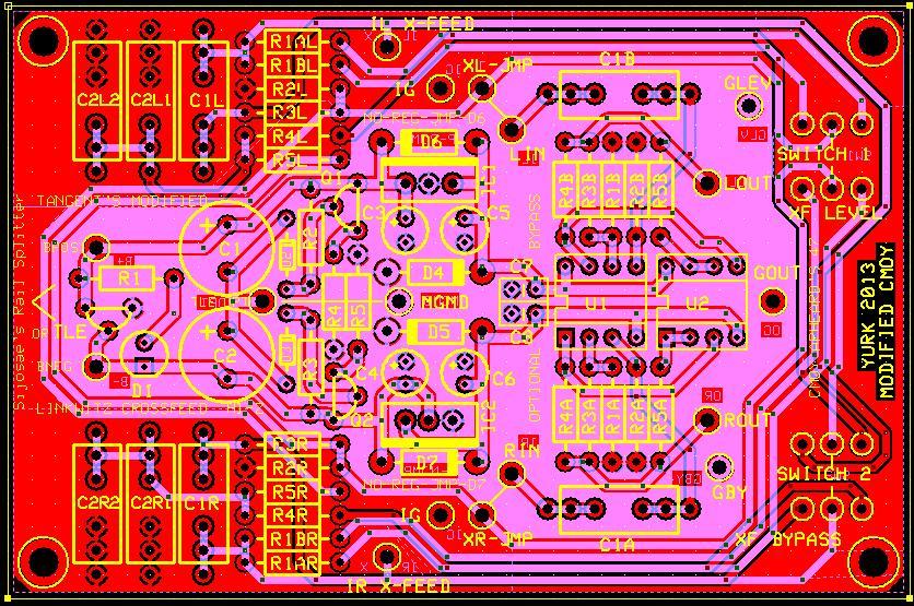
This is the part list that for this board. I do understand part of the schematics, and can see where most of the components go. But the wirepad list makes me scratch my ears...
Partlist
Exported from CMOY.sch at 10/24/13 9:45 AM
EAGLE Version 6.5.0 Copyright (c) 1988-2013 CadSoft
Assembly variant:
Part Value Device Package Library Sheet
BNEG 2,54/1,54 2,54/1,54 2,54/1,54 wirepad 1
BPOS 2,54/1,54 2,54/1,54 2,54/1,54 wirepad 1
C1 470uF CPOL-USE5-10.5 E5-10,5 rcl 1
C1A 0.47uF C-US150-054X183 C150-054X183 rcl 1
C1B 0.47uF C-US150-054X183 C150-054X183 rcl 1
C1L 0.022uF C-US150-054X183 C150-054X183 rcl 1
C1R 0.022uF C-US150-054X183 C150-054X183 rcl 1
C2 470uF CPOL-USE5-10.5 E5-10,5 rcl 1
C2L1 0.1uF C-US150-054X183 C150-054X183 rcl 1
C2L2 0.022uF C-US150-054X183 C150-054X183 rcl 1
C2R1 0.1uF C-US150-054X183 C150-054X183 rcl 1
C2R2 0.022uF C-US150-054X183 C150-054X183 rcl 1
C3 4.7uF CPOL-USE2.5-5 E2,5-5 rcl 1
C4 4.7uF CPOL-USE2.5-5 E2,5-5 rcl 1
C5 10uF CPOL-USE2.5-5 E2,5-5 rcl 1
C6 10uF CPOL-USE2.5-5 E2,5-5 rcl 1
C7 0.1uF C-US025-025X050 C025-025X050 rcl 1
C8 0.1uF C-US025-025X050 C025-025X050 rcl 1
D1 GREEN LED5MM LED5MM led 1
D2 1N4148-3 1N4148-3 1N4148-3 diode 1
D3 1N4148-3 1N4148-3 1N4148-3 diode 1
D4 1N4004DO14_10A 1N4004DO14_10A DO41_10A diode 1
D5 1N4004DO14_10A 1N4004DO14_10A DO41_10A diode 1
D6 1N4004DO14_10A 1N4004DO14_10A DO41_10A diode 1
D7 1N4004DO14_10A 1N4004DO14_10A DO41_10A diode 1
GBY 2,54/1,54 2,54/1,54 2,54/1,54 wirepad 1
GIN 2,54/1,54 2,54/1,54 2,54/1,54 wirepad 1
GLEV 2,54/1,54 2,54/1,54 2,54/1,54 wirepad 1
GOUT 2,54/1,54 2,54/1,54 2,54/1,54 wirepad 1
IC1 7812TV 7812TV TO220V linear 1
IC2 7912 79 TO220V linear 1
IG 2,54/1,54 2,54/1,54 2,54/1,54 wirepad 1
IL 2,54/1,54 2,54/1,54 2,54/1,54 wirepad 1
IR 2,54/1,54 2,54/1,54 2,54/1,54 wirepad 1
LIN 2,54/1,54 2,54/1,54 2,54/1,54 wirepad 1
LOUT 2,54/1,54 2,54/1,54 2,54/1,54 wirepad 1
MGND 2,54/1,54 2,54/1,54 2,54/1,54 wirepad 1
OPT 2,54/1,54 2,54/1,54 2,54/1,54 wirepad 1
Q1 2N3904 MPS8099 TO92-8099 transistor 1
Q2 2N3906 MPS8599 TO92-8099 transistor 1
R1 10k R-US_LEACH_0.4_RES LEACH_0.4_RES resistor 1
R1A 4.7K R-US_LEACH_0.4_RES LEACH_0.4_RES resistor 1
R1AL 2K R-US_LEACH_0.4_RES LEACH_0.4_RES resistor 1
R1AR 2k R-US_LEACH_0.4_RES LEACH_0.4_RES resistor 1
R1B 4.7K R-US_LEACH_0.4_RES LEACH_0.4_RES resistor 1
R1BL 1.5K R-US_LEACH_0.4_RES LEACH_0.4_RES resistor 1
R1BR 1.5k R-US_LEACH_0.4_RES LEACH_0.4_RES resistor 1
R2 4.7K R-US_LEACH_0.4_RES LEACH_0.4_RES resistor 1
R2A 100K R-US_LEACH_0.4_RES LEACH_0.4_RES resistor 1
R2B 100K R-US_LEACH_0.4_RES LEACH_0.4_RES resistor 1
R2L 1K R-US_LEACH_0.4_RES LEACH_0.4_RES resistor 1
R2R 1K R-US_LEACH_0.4_RES LEACH_0.4_RES resistor 1
R3 4.7K R-US_LEACH_0.4_RES LEACH_0.4_RES resistor 1
R3A 10K R-US_LEACH_0.4_RES LEACH_0.4_RES resistor 1
R3B 10K R-US_LEACH_0.4_RES LEACH_0.4_RES resistor 1
R3L 9.1K R-US_LEACH_0.4_RES LEACH_0.4_RES resistor 1
R3R 9.1K R-US_LEACH_0.4_RES LEACH_0.4_RES resistor 1
R4 10 R-US_LEACH_0.4_RES LEACH_0.4_RES resistor 1
R4A 47 R-US_LEACH_0.4_RES LEACH_0.4_RES resistor 1
R4B 47 R-US_LEACH_0.4_RES LEACH_0.4_RES resistor 1
R4L 3.3K R-US_LEACH_0.4_RES LEACH_0.4_RES resistor 1
R4R 3.3K R-US_LEACH_0.4_RES LEACH_0.4_RES resistor 1
R5 10 R-US_LEACH_0.4_RES LEACH_0.4_RES resistor 1
R5A 47 R-US_LEACH_0.4_RES LEACH_0.4_RES resistor 1
R5B 47 R-US_LEACH_0.4_RES LEACH_0.4_RES resistor 1
R5L 3.3K R-US_LEACH_0.4_RES LEACH_0.4_RES resistor 1
R5R 3.3K R-US_LEACH_0.4_RES LEACH_0.4_RES resistor 1
RIN 2,54/1,54 2,54/1,54 2,54/1,54 wirepad 1
ROUT 2,54/1,54 2,54/1,54 2,54/1,54 wirepad 1
S1L1 2,54/1,54 2,54/1,54 2,54/1,54 wirepad 1
S1L2 2,54/1,54 2,54/1,54 2,54/1,54 wirepad 1
S1L3 2,54/1,54 2,54/1,54 2,54/1,54 wirepad 1
S1R1 2,54/1,54 2,54/1,54 2,54/1,54 wirepad 1
S1R2 2,54/1,54 2,54/1,54 2,54/1,54 wirepad 1
S1R3 2,54/1,54 2,54/1,54 2,54/1,54 wirepad 1
S2L1 2,54/1,54 2,54/1,54 2,54/1,54 wirepad 1
S2L2 2,54/1,54 2,54/1,54 2,54/1,54 wirepad 1
S2L3 2,54/1,54 2,54/1,54 2,54/1,54 wirepad 1
S2R1 2,54/1,54 2,54/1,54 2,54/1,54 wirepad 1
S2R2 2,54/1,54 2,54/1,54 2,54/1,54 wirepad 1
S2R3 2,54/1,54 2,54/1,54 2,54/1,54 wirepad 1
TLE TLE2426CLP TLE2426CLP TO226AA tle2426 1
U1 OPA2132P OPA2132P DIL08 burr-brown 1
U2 OPA2132P OPA2132P DIL08 burr-brown 1
XL-JMP 2,54/1,54 2,54/1,54 2,54/1,54 wirepad 1
XR-JMP 2,54/1,54 2,54/1,54 2,54/1,54 wirepad 1
First of all this thread title really should be changed to Crazy A47 board. If the mods don't see this post I'll send a report.
That is a CAD-generated component list. The wirepads listed look to be jumper wires and connections for the offboard components. For example, this
I need to gather all the schematics and have a look to figure it all out, but that won't be until after I get some shuteye. It's 2AM here.
That is a CAD-generated component list. The wirepads listed look to be jumper wires and connections for the offboard components. For example, this
would be where the DC power supply connects, and thisBNEG 2,54/1,54 2,54/1,54 2,54/1,54 wirepad 1
BPOS 2,54/1,54 2,54/1,54 2,54/1,54 wirepad 1
would be Input Ground, Input Left, and Input Right respectively.IG 2,54/1,54 2,54/1,54 2,54/1,54 wirepad 1
IL 2,54/1,54 2,54/1,54 2,54/1,54 wirepad 1
IR 2,54/1,54 2,54/1,54 2,54/1,54 wirepad 1
I need to gather all the schematics and have a look to figure it all out, but that won't be until after I get some shuteye. It's 2AM here.
Sounds stupid, but i already have a hard time finding the drilled holes for the battery...
The battery holes are on the left at the rail splitter) and are labeled BPOS and BNEG
I like it!
I'd suggest having a look at Diptrace, it has a free edition, and I've found it to be very intuitive to use. Much much more so than EAGLE.
I use iteadstudio for my prototypes, they're very competitive priced, and make pretty high quality boards to boot
Peace
chris
I'd suggest having a look at Diptrace, it has a free edition, and I've found it to be very intuitive to use. Much much more so than EAGLE.
I use iteadstudio for my prototypes, they're very competitive priced, and make pretty high quality boards to boot
Peace
chris
- Status
- This old topic is closed. If you want to reopen this topic, contact a moderator using the "Report Post" button.
- Home
- Amplifiers
- Headphone Systems
- Crazy CMOY board