Amperage,
For proper ferrite beads implementation check this out:
http://s3t.it/data/uploads/dac_1541_v011.png
(at least i think it is proper way)
The 20v connector on the left - all the conductors pass thru ferite beads, GND and supply wires, and there is a ground fill cutout around "dirty" side - so the RF won't go to the board thru parasitic capacitance.
Amperage,
For proper ferrite beads implementation check this out:
http://s3t.it/data/uploads/dac_1541_v011.png
(at least i think it is proper way)
The 20v connector on the left - all the conductors pass thru ferite beads, GND and supply wires, and there is a ground fill cutout around "dirty" side - so the RF won't go to the board thru parasitic capacitance.
Looks good.. Your design?
I have ferrites on every line except the power ground currently (ran out). I have more suitable ones on the way here that work better around the 1ghz mark along with a bunch of those X2Y caps in 22pf, 100pf and 0.1uf.
Got the 100pf for peak performance around the 800-900mhz range and the 22pf extends nicely up to around 2ghz. The 0.1uf X2Y's will decouple the op amp power coming in from the 2mhz DC/DC converter to clean up any stray noise from that. I'll have a decade capacitor arrangement using normal ceramics along with the 0.1uf X2Y to help smooth things out a little more(1uf and 10uf).
I also ordered some teeeeeny carbide drill bits and some press in vias (ugh) to make stiching the ground planes together a bit more tolerable. Won't have to hand solder small bits of wire through each. I really need to setup something to plate my drilled pcbs

some possibly usefull links:
http://www.compliance-club.com/pdf/EMCTestingPart1.pdf
http://www.compliance-club.com/pdf/EMCTestingPart2.pdf
http://www.compliance-club.com/pdf/EMCTestingPart3.pdf
http://www.compliance-club.com/pdf/EMCTestingPart4.pdf
http://www.compliance-club.com/pdf/EMCTestingPart5.pdf
http://www.compliance-club.com/pdf/EMCTestingPart6.pdf
http://www.compliance-club.com/pdf/EMCTestingPart7.pdf
EMC Design
Design Techniques for EMC
Design Techniques for EMC: cables and connectors
EMC Compliance Club – Design Techniques for EMC. Part 3 — Filtering and Suppressing Transients.
Design Techniques for EMC - part 4
PCB DESIGN TECHNIQUES FOR LOWEST-COST EMC COMPLIANCE
Design for EMC Part 6: ESD, dips and dropouts, etc.
A lighter view, even though it mentions emissions the reverse is true.
The 10 Best Ways to Maximize Emission from Your Product
These devices get used a lot, especially where radio transmissions are used.
ACH32C-103
Put the name in google and you'll get the data sheet, the central GDN connection is connected either directly to the board GND, or on an isolated plane joining the main ground through a larger ferrite, both schemes get used and both work. Also sometimes they get used together, more delicate signals requiring the standard GND, power and more robust using the "dirty ground". These devices are also often used in conjunction with some ESD protection, to avoid nasty spike from the user when they plug something in or out.
Last edited:
It's a problem making good doublesided boards at home. I still make them, they have their place, but you just can't do as good a job as a PCB manufacturer unless you're prepared to virtually become a PCB manufacturer.
You can get 10 off 50*50mm boards delivered in ~10 days for $10 + postage from seeedstudio.com. Look under 'Services'.
You can get 10 off 50*50mm boards delivered in ~10 days for $10 + postage from seeedstudio.com. Look under 'Services'.
Last edited:
You can get 10 off 50*50mm boards delivered in ~10 days for $10 + postage from seeedstudio.com. Look under 'Services'.
$10 really? How can they afford that? Most places charge around $75 or so setup fee and to get to a reasonable cost per board you have to order 100+.
For troubleshooting and small modifications 10 day turnaround is still pretty annoying but $10.. that's cheap!
On the plus side I've got this LTE RF noise down to a dull roar so I think once I get my X2Y parts in and redo my layout for them I should be pretty solid.
Last edited:
$10 really? How can they afford that?
It is true. I had the board below made at iTeadstudio a couple of months ago. The pricing is similar to Seeedstudio and I think the two may use the same board house. Great quality. I paid $19 for 10 pieces of 80mm X 100mm boards (1.6mm, HASL, 2 layer, green), regular $24, a special they had going during the Chinese holiday. Then $20 DHL from China. The 4 day shipping cost more than the 10 boards. PCB prototyping
Attachments
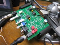
It is true. I had the board below made at iTeadstudio a couple of months ago. PCB prototyping
that's a handy looking vise you have there. did you modify another product or It came like that?
i'm not sure I would say its great quality, but its certainly very good for the money. if I was doing something for production I wouldnt use them, the screen printing and soldermask can be a little less than perfect sometimes and i'm not 100% sure they do 100% E-test/flying probe testing; but hey its $10!!. or even try seeed, which have the same $10 deal, plus $39 for 4 layer!! which may use the same boardhouse, but they seem to have even better deals. is it iTEAD that includes shape routing in the cost?
some of these services arent quick though, usually up to a few weeks, so doing stuff at home is better if you need to do a one off quickly, or perhaps a larger board, but really there is little reason to do a second generation board at home anymore
I say again $39 for 10 x 4 layer PCBs!!
some of these services arent quick though, usually up to a few weeks, so doing stuff at home is better if you need to do a one off quickly, or perhaps a larger board, but really there is little reason to do a second generation board at home anymore
I say again $39 for 10 x 4 layer PCBs!!
Last edited:
Yeah definitely worth it.. Once I get my final component list I'll probably do a 4 layer layout and get the 10 for $39 deal. I wonder if they allow you to panelize like iTead to squeeze more boards in for the size. the boards will end up being something like 80mm x 21mm so I could fit 4 boards in to a 10cmx10cm area.
you can panelize, but you have to cut them yourself. the $39 is for 50 x 50mm. if you actually need or want to panelize to 10x10cm and get 40 PCBs once youve cut it, you would need to add 50 bucks for $89. If 20 is enough, just get the $69 for 10 pieces of 10 x 5cm. since you are going for as good HF decoupling as you can, I recommend going with the thinnest PCB, which is 0.8mm. not as sturdy if that worries you, but decoupling is more effective, as is signal->ground closer and thus better.
Power and ground would be closer as well adding more planar capacitance.I recommend going with the thinnest PCB, which is 0.8mm. not as sturdy if that worries you, but decoupling is more effective, as is signal->ground closer and thus better.
If you want help panelising your Gerber data let us know, I have a the full CAM350, so can do panelisation (allows you to send one image) and do a quick manufacturers DFM to their capabilities, if they are listed (they usually are).
Marc
that's a handy looking vise you have there. did you modify another product or It came like that?
The vise is fantastic. It is Panavise 350:
https://panavise.com/index.html?pageID=1&page=full&--eqskudatarq=5
PanaVise 350 Multi-Purpose Work Center: Amazon.com: Industrial & Scientific
The 350 has jaws that go out to 220mm, big enough for a 160mm card, yet can flip around to hold very small boards. I bought a "Panavise Jr" first which proved to be useless for anything I work on. The base is too light and slides around. The base of the 350 is *heavy*. Stays put without mounting it to anything.
Very nice.. Thanks for the link. I see they have some accessories that work with that line of vises. I'll have to look around a bit and order me some new toys
.BTW I got a bunch of X2Y caps in today. still waiting on the new ferrites and some other stuff to build the new DC/DC converter but I'm gonna start on the new layout for the X2Y stuff and maybe attempt some via stitching ;( got some new 0.021" and 0.0138" carbide bits in today also. I wasn't able to find any via rivets that small but with a whole bunch of Dr. Pepper and a bit of a migraine I can probably get a test layout done with 5x5mm stitching using fine enamel wrapping wire to connect the via pads.
It will take hours to build the test board likely but at least I'll have an idea if the layout in general is usable to be sent off to a board house.
You can likely just literally use stitching, i.e. thread the tiny wire through a needle and just push it down through one hole and up through the next and keep going, leaving the wire between adjacent holes. Or do the same thing but without a needle. AFTER soldering, you could remove the wire between holes, if necessary. The main point is to not try to work with very short pieces of the tiny wire.
You can likely just literally use stitching, i.e. thread the tiny wire through a needle and just push it down through one hole and up through the next and keep going, leaving the wire between adjacent holes. Or do the same thing but without a needle. AFTER soldering, you could remove the wire between holes, if necessary. The main point is to not try to work with very short pieces of the tiny wire.
Thanks for the suggestion. I made a small jig to hold the boards and thread the wire along for me so I can feed the wire through the hole and have both hands free to solder them in place. Made things much easier.
Still waiting on the rest of my parts from mouser to get the new board layout tested for the larger amp.
Interestingly enough I redid the layout on my smaller amp and did nothing special to help with RF. It only has one ground plane with a few scattered vias from the component side. No RF filtering at all on the inputs and outputs and it's pretty quiet. Even with LTE it's only faint background noise that's drowned out by music at even very low volumes.
This is the new layout for the little amp. 130mW/channel 32ohm ~8 hour run time near 100% volume around 12h at more moderate levels with a 180mah li-po cell. 15 minute charge time from dead. The casing size is 1.8"x 1.2" x 0.5".
This layout isn't too bad RF noise wise. The 4 pads at the corners are just positioning markers for the 2 layers when I sandwich the PCB for toner transfer
An externally hosted image should be here but it was not working when we last tested it.
This layout isn't too bad RF noise wise. The 4 pads at the corners are just positioning markers for the 2 layers when I sandwich the PCB for toner transfer
Last edited:
Don't need thermal relief on vias.
Yeah those are actually hole through pads technically to the layout software. While thermal reliefs aren't needed on vias I prefer the software draws them on some connections.
After etching I hold the board up to the light and use the thermal reliefs like a crosshair to see if I was off and by how much on my layer alignment. Makes it easy to correct small offsets with drilling angle.
Some acid traps visible.
While T junctions and tight angles may not be the best practice I'm home etching with some pretty fine tracks (down to 0.15mm) and I get very clean results. Have never had bridges or incomplete etches because of it so I tend not to get overly worried about it. if it complicates layout or forces me to space pads further apart I generally just go for the T.
IF/When that particular layout goes to a board house I'll likely remove the thermal reliefs (I'd hope they can line up the layers) and they do no good on a professional board since I won't be manually soldering wires through the vias to bridge layers.
And I might rework some of the layout a bit to try and avoid some of the bigger acid traps.. after all who knows how well they rinse boards etc. I know I clean them well myself but that's me.
And I might rework some of the layout a bit to try and avoid some of the bigger acid traps.. after all who knows how well they rinse boards etc. I know I clean them well myself but that's me.
I forgot you were manually soldering the vias (Have fun)
The acid traps are not much of a problem these days as they use to be, often it is more for the appearance of the finished design, where the traces enters the large pad by the text 2K is an example.
Professional PCB manufacturers who make multi-layer boards must be able to line up the layers, and I can’t remember when I last had a layer alignment problem with a manufactured board, probably about 1988. They manufacture the boards in panels and will have tooling holes in the pre-pregs and laminates to align the layers before the mass lamination, and dependant on the board complexity may use other methods of ensuring alignment. I often have 10-16 layer design done with no problems.
If you haven’t already got this on your desktop, download it, it is an invaluable guide for various PCB related calculations.
Saturn PCB Design - PCB Via Current | PCB Trace Width | Differential Pair Calculator | PCB Impedance
- Status
- This old topic is closed. If you want to reopen this topic, contact a moderator using the "Report Post" button.
- Home
- Amplifiers
- Headphone Systems
- RFI problems on diy headphone amp.