Well a small update. I've tried all of the above suggestions.
10uf, 1uf and 0.1uf decoupling caps bridged right from the power pins on the op amp to ground for both + and - power supply lines (all 0603 SMD multi-layer X7R caps).
Ferrite beads on not only the audio inputs and outputs but also on the ground and +/- voltage source.
Shorted both non inverting inputs to ground right at the op amp to eliminate the entire input path.
Temporarily removed the 150pf caps from the feedback loops.
Lowered the gain to 6.
Nothing at all seems to affect the amount and loudness of the interference except the position of the phone relative to the board and cabling. Changing the gain, changing input ground path load resistor value, adding the T circuit to the headphone outputs.
One interesting thing I noticed is if I force my phone back to 3G data connection all the noise goes away. The amp is dead silent even laying right on the back of the cell phone so it appears the problem is limited to 4G at least in this case.
Is it possible that the noise I'm hearing from the 4g radio isn't actually high freq RF noise being demodulated but perhaps some other signal bleed actually in the audible range?
If that's the case no amount of filtering that doesn't impact the actual sound of the amp will remove it.
Last edited:
Nothing at all seems to affect the amount and loudness of the interference except the position of the phone relative to the board and cabling.
I think it's RF bursts (actually coded data, but for us it's the same) which within a certain small distance fom the antenna are strong enough to be rectified by *any* PN junction (of which there are tens to hundreds available inside any audio device); such complex shape pulses are wideband by definition, so filtering amounts to kill audio.Is it possible that the noise I'm hearing from the 4g radio isn't actually high freq RF noise being demodulated but perhaps some other signal bleed actually in the audible range?
If that's the case no amount of filtering that doesn't impact the actual sound of the amp will remove it.
Probably the only solution is to fully enclose the audio equipment in a Faraday cage ... and even so I suspect some strong RF will "travel back" through the earphone wires into the amplifier and be rectified ... in which case such "audio" will mix with the actual Music and be heard on the phones.
So far only defense against such interference is to move the transmitter away so induced voltage does not get rectified (<0.7V peak?)
I usually have my cellphone less than 2 Ft away from my CPU (which is *supposed* to be RF shielded such as to not leak digital noise outside) and I regularly hear through the PC speakers the "bzzt bzzt" sounds it makes every few minutes, probably the "I am still here" signal to the closest tower.
And it becomes crazy a few seconds *before* it starts ringing , so when it does I already have it in my hand.
I commented in other forums a very annoying "mystery" interference I had ***everywhere*** a few years ago.
Everywhere means Radio/TV/Phone/PC/anything.
My friends joked I would soon have it in the Fridge and washing machine
")
Sound was maddening : "silence for 40 seconds ... tick ... tick ... TICK ... BZZZZT .... BZZZT ... TICK ... tick ... silence .... "
One day a neighbour came and on hearing it commented: "are you repairing a Marine Radar?" (He's a ship Captain).
That solved the mystery.
I live in the old Buenos Aires port, less than 80 meters from the riverside, and they were repairing a Spanish fishing ship, anchored "at the corner of my house".
Looks like Ship Radars have 2 settings: "sailing" (full power) and "Port" (5W average)", because they need to "see" at most 200 meters away ... and they were (illegally) using it full power.
The ticking sound was the transmitted pulse, and the 40 seconds silence was when the antenna rotated away.
Last edited:
afaik, its a ping, I used to get it in 2 situations, when the phone was just about to receive, or send a call/message, or when the phone was forced to switch to 2G when it pinged the nearest tower. I moved to balanced portables, nothing just pure audio bliss now . there are other ways to tackle it, some amps are more affected than others, but balanced is an excellent cheat, if a bit pricey, as it wont work with just using a phase splitter unless its entering the circuit after the conversion to balanced; so you need a balanced dac too. otherwise I would suggest just swapping to something like an OPA1632 or THS4521, which take single ended input and output balanced.
. there are other ways to tackle it, some amps are more affected than others, but balanced is an excellent cheat, if a bit pricey, as it wont work with just using a phase splitter unless its entering the circuit after the conversion to balanced; so you need a balanced dac too. otherwise I would suggest just swapping to something like an OPA1632 or THS4521, which take single ended input and output balanced.That's a pretty sharp cut in max power output but if nothing else I try helps that's something not too difficult or expensive to try.
Here is a solution that I first leaned about from jcx here a couple of years ago, figure 1:
http://www.intersil.com/content/dam/Intersil/documents/an11/an1111.pdf (opens PDF)
puts the second half of the OPA2132 in parallel with the first to nearly double the output current to 60 - 80 mA, right up there with one section of the NJM4556A. 1 ohm should work for the two output balancing resistors (Rbm1 and Rbm2), giving you just 0.5R output impedance looking back into it. You could just use a quad OPA4132, but I wouldn't recommend it for power dissipation reasons. Probably best to use two OPA2132s, one for each channel. The slight time delay through the second chip should be insignificant for audio.
Interesting about the tests! Here is another test to try. Tinfoil hat time.
Cut a square of aluminum foil about 1 inch wider than your PC board in both directions, then put strips of 2 or 3 inch wide packing tape or duct tape on one side of the foil to insulate it. Then ground one corner with a test clip and just set the thing right on top of the PCB, insulated side down of course, and move the phone above the foil. If that helps, try cutting the foil square down smaller and smaller until it is just right above the chip and see how it goes. The RF can still get in under the edges, but the foil should cut the field strength down substantially if the problem is directly radiated energy into part(s) and/or PCB traces (as opposed to off-board wiring).
Last edited:
Cell phones are a PITA. The only practical solution is to physically move the phone away from the amp. Trust me,I've pulled my hair out trying to kill cellphone RFI - it ain't happenin. Certain phones/providers seem to be worse than others.
(I've never had this issue with my own cellphones,but I use an older non-smartphone,and the basic calling plan,no data or other BS.)
The problem is that it's pulsed data,big nasty square wave pulses,with harmonics as far as the eye can see.
(I've never had this issue with my own cellphones,but I use an older non-smartphone,and the basic calling plan,no data or other BS.)
The problem is that it's pulsed data,big nasty square wave pulses,with harmonics as far as the eye can see.
Noise Suppressing Sheets / Magnetic Sheets | Products - TDK
I have seen some of this TDK stuff attenuate a GSM signal more than a few dB with just a single sheet. The problem is it is very expensive, I think $75-100 per sq ft and it's not a sure thing depending on the mode of coupling.
You can try Laird HF ferrites, normal ferrites are useless at these frequencies. You can also try an X2Y C0G cap as an input filter.
if phone has low signal, it can transmit up to 2W to antenna. that is quite a lot of energy radiatedBoth amplifiers are nearly silent almost no hiss or other odd noises I can attribute to the amplifiers themselves and I'm quite happy with the audio quality but I've been having persistent issues with RFI from my 4g cell phone when it's transmitting or receiving data within approximately 1 foot of either headphone amp.
learn to live with it
Well if it's some type of low frequency pulses being sent as a result of the radio equipment in the phone changing power levels etc then I guess there isn't much I'm going to do about it other than move the phone further away or move to a better signal area
I'll play around with the grounded aluminum foil idea a bit. maybe ground to some water lines to test.
The amp that has the cell phone noise issues is inside a full aluminum shell with only openings for plugs and controls and is grounded to the PC chassis while plugged in charging but computer grounds are far from ideal. It's not like I can keep a portable amp earth grounded but just out of curiosity I'll give it a shot.
I'm also tempted to order a FiiO E6 and see if it's really immune to the issue or if perhaps the reviewer forgot to take his phone off of airplane mode.
It's in a plastic housing and from what I can tell by the pics I can see of the PCB it doesn't use any type of crazy chokes etc but if I had one to look at here and it's not affected by my noise problem it wouldn't be hard to study the board and see how they solved the puzzle.
I would have ordered one just to play with already but I've read some negative comments about build durability on it and I wanted to build an amp with enough voltage swing to drive 600ohm cans if need be. Also my amp lets me still use the in-line mic/remote controls on the headphones that have them. AFAIK most retail amps only have TRS (3 conductor) jacks and/or won't pass through the sleeve connection untouched.
Anyone reading this that has a FiiO E6 if you could sandwich it against your cell phone and see if any noise creeps through while the phone is transmitting that would be awesome (4g data connection preferably).
I'll play around with the grounded aluminum foil idea a bit. maybe ground to some water lines to test.
The amp that has the cell phone noise issues is inside a full aluminum shell with only openings for plugs and controls and is grounded to the PC chassis while plugged in charging but computer grounds are far from ideal. It's not like I can keep a portable amp earth grounded but just out of curiosity I'll give it a shot.
I'm also tempted to order a FiiO E6 and see if it's really immune to the issue or if perhaps the reviewer forgot to take his phone off of airplane mode
. It's in a plastic housing and from what I can tell by the pics I can see of the PCB it doesn't use any type of crazy chokes etc but if I had one to look at here and it's not affected by my noise problem it wouldn't be hard to study the board and see how they solved the puzzle.
I would have ordered one just to play with already but I've read some negative comments about build durability on it and I wanted to build an amp with enough voltage swing to drive 600ohm cans if need be. Also my amp lets me still use the in-line mic/remote controls on the headphones that have them. AFAIK most retail amps only have TRS (3 conductor) jacks and/or won't pass through the sleeve connection untouched.
Anyone reading this that has a FiiO E6 if you could sandwich it against your cell phone and see if any noise creeps through while the phone is transmitting that would be awesome
(4g data connection preferably).
Last edited:
Thing us at cell phone frequencies it only takes a inch of wire to present significant impedance, earthing as such is not helpful.
Ensuring all connectors are bolted directly to the box, have 100pf caps across them right at the box (SMT ceramic MLCC is better then leaded disk) and have some inductance in the lines to the board will usually make it go away. Common impedance coupling is the kiss of death for immunity, and there is much to be said for using a 4 layer board to allow a continious ground plane.
Dont forget that pickup in the output wiring can be every bit as troublesome as pickup in the inputs,but with appropriate design and layout cell phones can be beaten.
Regards, Dan.
Not my best picture, but you should be able to make out what it is, a small copper box, 22.5*30mm, intended for RF applications. You need to leave mounting holes in the PCB, and exposed copper on the PCB around the periphery of the box to allow a solder bead to be run all the way round the box to connect to the ground plane. If you have a ground plane on the bottom of the board, you need to take numerous vias from top to bottom (stitching) anywhere there are no traces.
These are obviously used to surround sensitive (or emitting, such as an LO) parts of the circuit.
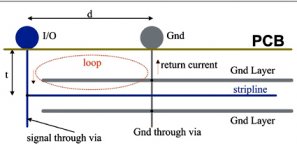
If the best isolation is required, a multi-layer PCB with planes on top and bottom is used, and traces taken to the components on the inner layers, stripline (embedded controlled-impedance trace) would be employed in the case of RF circuits.
You need to get your beads right up against the box if you use a doublesided board (although obviously not shorting to it), diving the traces through a gap in the solder bead, or as close to the component pins as possible if no box is used, they're not helping much where you've got them.
These are obviously used to surround sensitive (or emitting, such as an LO) parts of the circuit.
An externally hosted image should be here but it was not working when we last tested it.
If the best isolation is required, a multi-layer PCB with planes on top and bottom is used, and traces taken to the components on the inner layers, stripline (embedded controlled-impedance trace) would be employed in the case of RF circuits.
You need to get your beads right up against the box if you use a doublesided board (although obviously not shorting to it), diving the traces through a gap in the solder bead, or as close to the component pins as possible if no box is used, they're not helping much where you've got them.
Last edited:
Hey, don't forget the cellphone already has DAC and tiny headphone amp INSIDE, which isn't prone at all to the EMI agressor located SO CLOSE.
It's just the layot bug somewhere.
Get ferrite clamps/rings and put 'em on all the wires...
Oddly enough the energy causing the noise seems to be very directional. if I move the phone around across the PCB I can hear the noise shifting back and forth between left and right channels in the headphones and if I run the phone along the length of the headphone cable I can hear the noise but only in certain spots along the cable. if I took the time to measure it carefully there would probably be a pattern as far as the locations in the cable where it's picking up the loudest.
if I hold the phone at certain angles relative to the pcb the noise almost completely vanishes so it's not being radiated evenly around the phone. If one knew enough about the signal itself it might be possible to place sensitive electronics in a "dead spot". Of course I don't have that luxury with something I just toss in my pockets along with the phone
You need to get your beads right up against the box if you use a doublesided board (although obviously not shorting to it), diving the traces through a gap in the solder bead, or as close to the component pins as possible if no box is used, they're not helping much where you've got them.
I had no idea ferrite bead placement was so sensitive. I just put them right at the input and output pins and ground filled around them.
I'm somewhat limited on the other aspects you mentioned like affording a full unbroken ground plane on both sides of the signal layers because I'm making the boards at home and guessing at a 4 layer design to have manufactured with a 2 week turnaround and high setup costs wouldn't really be worth the investment time or otherwise specially when I could get the boards back and still have the issue even with the 4 layer design and signal layers fully sandwiched between shielding layers.
Last edited:
Just as a suggestion, the top ground plane has several loops in it and these can act as antennas as well.
You might try separating these into sections that are by themselves with only one connection per section to the bottom ground plane.
I read up on this a while back but I don't have a link to post for you as it was about having ground planes in audio circuit's create more havoc than what is realized.
Unless they are done correctly.
Typically most are done with cross hatch patterns as well, with the top going one way and the bottom plane going the other way.
If they weren't their at all there would be no antenna actions to be picking up the RF and inducing it to the amplifier's traces, and, the box itself would be doing all/most of the shielding from the outside EMI.
Typically soft steel is used to shield RF.
One time I was building an RF power amp out of a MRF455 and I had a Ferrite bead feeding the bias resistor to the base from ground and this actually caused the thing to be a 50watt oscillator.
I removed the bead from the resistor and base and it worked perfectly as I had intended it to be with no other changes.
These are tough things to figure out at times.
Check the integrity of your power supply as well.
I have an old regulated supply that I found likes to oscillate at about 450Khz whenever I bypass the opamp that it is powering with a .1uf capacitor.
Adding a 100uf capacitor across the output on the supply board solved that issue.
Except now only one time so far I have caught it oscillating a 710Khz and I don't know why this is.
It has only done it once so far and it stays on 24/7 with the opamp connected.
My scope is connected to the outputs of the opamp and is on 24/7 as well, that is how I caught it.
After turning the power supply off and then back on again it stopped and has yet to do it again in the last two days.
Go Figure?!!!!
FWIW
jer
Just as a suggestion, the top ground plane has several loops in it and these can act as antennas as well.
You might try separating these into sections that are by themselves with only one connection per section to the bottom ground plane.
I read up on this a while back but I don't have a link to post for you as it was about having ground planes in audio circuit's create more havoc than what is realized.
Unless they are done correctly.
Typically most are done with cross hatch patterns as well, with the top going one way and the bottom plane going the other way.
If they weren't their at all there would be no antenna actions to be picking up the RF and inducing it to the amplifier's traces, and, the box itself would be doing all/most of the shielding from the outside EMI.
Typically soft steel is used to shield RF.
So you are thinking the ground fill around the signal lines could actually be causing or at least contributing to the problems?
I could just eliminate the ground fill around on the component layer and leave the nearly solid ground plane on the other side then use via type jumpers to connect to that ground layer where needed.
Check the integrity of your power supply as well.
The circuit is currently being powered by a pair of 3.7v li-po cells for +/- 3.7v. The first thing I did for troubleshooting was remove everything that could be adding to the noise except the audio section from the equation and I can't get rid of the power for the op amp totally so a pair of li-po cells was as basic and neutral a power source as I could think of.
Some further experimenting yielded interesting results. I foil wrapped the entire circuit (batteries included). Nothing plugged into the input jack. the only exposed cable was the headphone cable then I grounded the foil.
This reduced the noise from the cell radio only slightly but still easily loud enough to be audible during music playback.
So I figure that has to be almost all going back to the circuit from the headphones so I unplug the headphones and plug the output into my computer's microphone input using a very short (6 inch) well shielded cable then I crank the gain up on the computer till I hear some hiss and turn the cell radio back on.. bzzt bzzt bzzt.. bop bop.
Ok noise is still there but I have no reference for if it's been reduced at all compared to when the headphones were plugged in. I don't have a oscope or meter that's fast enough to capture the peak voltage output accurately but the noise is still there.
So then I unplug the batteries from the op amp circuit and plug it back into the computer... hrmm. while it isn't amped as much the noise is still there so my circuit even unpowered is demodulating the cell phone signal into the computer's mic input.
Next thing I tried was to pop the op amp out of it's socket then held the phone next to the board again.. No noise.. nothing at all. Even with the mic input gain up as far as it can go I can hear white noise but nothing from the cell phone.
So basically even unpowered my amp circuit is working like a antenna but removing the op amp itself from the socket breaks the antenna.
The other thing I noticed is that you don't have a resistor feeding the +input of the opamp.
I duplicated your circuit configuration on my protoboard and it seems to be functioning fine.
But in this configuration the impedance at the + input will be extremely high and very sensitive to very low level signals.
The gain was very high as well but I didn't check to see what it was.
Have you tried putting a resistor series with the input capacitor and the +input?
I will have another look at this a little later as I didn't try to bring a cell phone or even my wireless phone near the circuit.
I figured I had plenty of noise floating around my bench I didn't see anything abnormal using my scope.
The opamp I am using is a JRC4560 and a TL082 on a single ended 12V supply using two 1k resistors as a virtual ground.
A very common setup.
I will see if I can find the info on ground planes for you.
jer
The other thing I noticed is that you don't have a resistor feeding the +input of the opamp.
I duplicated your circuit configuration on my protoboard and it seems to be functioning fine.
But in this configuration the impedance at the + input will be extremely high and very sensitive to very low level signals.
The gain was very high as well but I didn't check to see what it was.
Have you tried putting a resistor series with the input capacitor and the +input?
There is a 10k alps potentiometer immediately after the input ferrite beads and before the dc blocking capacitor. I don't have any series resistance to the + input after the cap. I can insert a resistor easy enough after the cap and before the grounded resistor and cap. I have a pretty low value resistor (2.2k) between the + input and ground. Most designs I've seen use a higher value but I had 5mv at the + pin using 100k and with a gain of 11 resulted in a very high 55mv DC at the headphones so I lowered that to 2.2k to get roughly 2-3mv offset at the output.
Also I haven't had interference problems from anything else. I tried holding the board next to my Wi-Fi router. a running microwave oven. near a AM/FM transmitter and even the phone on 3g seems fine. I only hear the noise when the phone is using 4g data connection.
Last edited:
I inserted a 4.7k ohm resistor immediately after the cap on the 2 inputs and increased the value of the loading resistors from 2.2k to 10k so the series resistor didn't drop the input voltage swing too much. No difference on interference.
I also inserted another 4.7k resistor between the + and - voltage rails to ground. no effect on noise although it did waste a bit more power
I also inserted another 4.7k resistor between the + and - voltage rails to ground. no effect on noise although it did waste a bit more power
Last edited:
Hmmmm....I don't have any of those types of signals to introduce.
I am thinking that if you have several points connecting the top plane with the bottom plane this would cause a grond loop and may be were the noise is being introduced at.
each plane should only have one connection point preferably closest to the grounded end of the bypass capacitors.
Also you want all of your signal paths as short as possible and not looped around the board crossing themselves along the way.
You must follow a star type pattern of grounding system.
Try disconnecting the top plane from the bottom all together and see if the noise goes away.
Here are a few links that may help you as I am still looking for one in general,
http://www.ultracad.com/articles/loop.pdf
- What is ground loop and how to prevent?
http://www.analog.com/library/analogdialogue/archives/43-09/EDch 12 pc issues.pdf
http://www.celectronics.com/seminar/sample/IEEE11-9-05.pdf
jer
Attachments
Last edited:
I am thinking that if you have several points connecting the top plane with the bottom plane this would cause a grond loop and may be were the noise is being introduced at.
Hrm. there isn't many connections between the 2 ground planes as is. basically just the connections for the ground and shielding on the headphone jacks. one via to connect an isolated patch that got trapped between some traces and the ground point for the power supply.. In any case I took a small blade and cut the connecting spokes for all the leads passing through the board on the non-component side so it's only connected now right at the power supply ground point and I bridged the little isolated D shaped patch on the right side using a component side jumper so now only 1 electrical connection to the red colored ground plane in the earlier forum pics.
I can still try segmenting the component side ground fill more and having all the pieces meet at the single power supply ground that will take some fancy dremel work
. I'd rather not make another board just for that
Last edited:
- Status
- This old topic is closed. If you want to reopen this topic, contact a moderator using the "Report Post" button.
- Home
- Amplifiers
- Headphone Systems
- RFI problems on diy headphone amp.