Whoops – that’s not an O2 Desktop Amplifier! After some reflection I fear that I’ve strayed from RocketScientist’s published design philosophies in his O2 headphone amplifier blog and posts here, which was sort of the whole point of this project to take a guess at what he might have put in his O2 Desktop Amplifier.
Specifically, from RocketScientist's writings:
And roll in some of my goals for this amp to slightly improve over the O2 amp and make it more of a desktop headphone amp:
So below is yet another project reboot.")
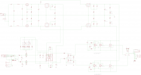
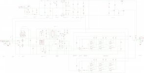
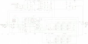
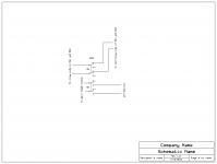
OUTPUT STAGE AND PROTECTION RELAY
POT AND COUPLING CAP IN THE MIDDLE
GAIN STAGE
POWER SUPPLY AND CASE
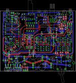
Clicking on the arrows in the lower left of the schematic will expand it. I haven't added the relay control circuit yet and haven't designed the clipping indicator circuit yet. Both will probably go on the back as SMD.
Specifically, from RocketScientist's writings:
- · Separate gain and output stages, with only local feedback in the stage. No global feedback of the gain loop to maximize stability. The gain chip can be a low-current low-noise low-distortion variety.
- · Pot in the middle to minimize resistor noise amplification and cap in the middle to block DC output offset voltage from the first stage, especially as the gain is increased.
- · Low cost! If there is a choice between a higher priced chip with minimal expected performance gains and a lower cost one, pick the lower cost chip. Any improvements have to justify the cost by making a fairly significant difference audibly or in the engineering parameters.
And roll in some of my goals for this amp to slightly improve over the O2 amp and make it more of a desktop headphone amp:
- · Much lower DC output offset voltage than the 3mV typical with the O2 headphone amplifier. Might matter to some very sensitive IEMs.
- · Lower input HPF corner frequency than the 10Hz of the O2 (bigger coupling caps). Probably no audible difference.
- · Lower ripple and noise power supply.
- Heat sinking the regulator chips.
- · Clipping indicator
- · Output relay on the headphones to delay turn-on by 2 seconds.
- Add the option of signal attenuation at 1X.
- · …and the possibility of lower distortion by using "better" chips rated as such, vs. the original O2 amplifier chipset, but we’ll never know until I can get access to a AP or dScope to properly test it.
So below is yet another project reboot.
OUTPUT STAGE AND PROTECTION RELAY
- · OPA827 wrapped around a LME49600 buffer, but now only unity gain in the local feedback loop which works since the OPA827 is unity gain stable (so is the OPA627 for that matter). Just like the O2, this one’s output stage is 1x for maximum stability and minimum amplification of noise in the pot or input bias ground return resistor. In the case of the OPA627 the datasheet shows that running at 1x gain results in a whole order of magnitude improvement in the THD vs. frequency, so I’m going to make the assumption (which may not be valid without measuring!) that the OPA827 is the same or better since the chip is supposed to be an upgrade.
- · Using the OPA827 is a concession to RocketScientist’s low costs design philosophy point above. The offset voltage the OPA827 will produce is already so low it will be irrelevant for any headphone or IEM. The OPA627 has trimmer pins that work well, I’ve found with my V1.0 PCB, to null that offset out even lower. But that version of the OPA627 is 3x the cost of the OPA827, so the even lower DC offset doesn’t justify the cost. HOWEVER, I have some OPA627 DIP8 chips and I personally would like that trimmer null, so I’m compromising by allowing either one to be used. J I’ve laid out the pad for a DIP8 socket, for the OPA627, right on top of and MSOP pad for the SMD DGK version of the OPA827. To use the OPA627 solder in the DIP 8 socket and the trimmer and 2 resistors, otherwise leave all that off and just solder the MSOP OPA827 right down to the board. This saves the cost and capacitance/inductance of using a Brown Dog adapter.
- · Related to the point above, the THD of both the OPA827 and LME49600 will worse as frequency goes up in the typical fashion for all op amps, of course. The (audio band) worst case THD of the OPA827 is 0.0002 at 20kHz from the data sheet. The LME49600 doesn’t publish that graph, but some data sheet diving in the tables has the THD at 20kHz listed at 0.0005 which can be presumed then to be the worst in the audio range. So that still makes the LME49600 the limiting factor on THD. The 0.0003 number of the OPA627 is still 60% better. RocketScientist made a big deal about the THD of the NJM4556A chips being the limiting factor and essentially swamping that of the lower distortion NJM20568 gain chip. That is a little less true here for the output stage since the OPA827 is wrapped around the LME49600 in the output stage and can serve to help further linearize the LME49600’s distortion if the input opamp has better specs like this.
- · Output LME49600 is properly faster than the OPA627 op amp for this type of design for maximum stability.
- · The FET input on the OPA827 is still useful, even though the cap in the center renders its low current draw kind of pointless for pot wiper DC, due to the reduced voltage drop created across the 100k input bias ground return resistor, and due to the highly imbalanced impedances looking out the inverting (0R) and non inverting (100k) pins. Matters less with 5pA input current.
- · Both a 3.5mm Switchcraft and ¼” Neutrik output jack both on the front panel for both types of headphone plugs.
- · Protection relay added on the headphone output, one of the O2 amplifier mods I posted that has worked extremely well in real life. 2 second amp turn on delay to connect the headphones plus an accelerated disconnect of the phones on amp turn-off. The relay circuit does not detect overvoltage (DC offset) since the assumption is that if a power supply rail dies, or an output chip dies, it would take out the relay control circuit too which is powered off the same rails. Wouldn’t work.
POT AND COUPLING CAP IN THE MIDDLE
- · Pot back to being in the center so the following buffer stage doesn’t amplify resistor noise.
- · A pad for an attenuation resistor is now in series with each pot feed. I find that I need 10k in series with the 10k pot to knock my sources down 50%. To keep load on the gain chip the same as the O2 amplifier, a 10k pot is used if the attenuation resistor is shorted (0R jumper resistor), while a 5k pot is used along with a 5k-or-so attenuation resistor for a total load on the gain chip still of around 10K.
- · Cap back in the center to block output offset voltage from the input gain stage. The first stage (gain) chip is now assumed to be something that doesn’t have to have very low input offset voltage and input bias current, but rather can be a bipolar that is more optimized for audio with gain.
GAIN STAGE
- · Since the coupling cap in the middle is back, the gain stage can be audio-optimized again and doesn’t have to have the DC precision numbers on offset and input bias current of the OPA627. So I’ve picked the metal can TO99 version of the LME49720 (LME49720HA) to replace the NJM2068 in the O2. This chip might have at least a possibility of a small improvement in parameters if properly measured, although as with the O2 the output stage distortion will swamp those numbers making it kind of pointless. But I’m making an exception to RocketScientist’s super low cost philosophy here just because the cost difference is so small. $6 for the TO99 LME49720 these days. I spent that much at Starbucks this morning. J Not in the same league as the $20 difference between the OPA827 and OPA627 high grade chips on the output (times two chips).
- Walt Jung once wrote that the National Semiconductor audio team had just started researching why the metal can versions of op amps were often reported to sound better when National shut the group down. I've been wanting to try a TO99 for awhile.
- · Still has the rotary gain switch that can be set up for 4 gain settings including 1x. I need attenuation, not gain, for my sources but I’m coming to realize from various posts that people really do use 6x and 8x with some iPods and other portable players.
- · RCA inputs in the back of the case and 3.5mm input plug in front.
- I've left a 15uF bank of three film capacitors on the input of each channel to keep DC out of the gain stage. Input DC would not affect the output due to the coupling cap being back in the middle, but it would shift the DC level of the input stage and can cause clipping or even damage the chip depending on voltage level. Just seems prudent to me to have DC blocking. 15uF puts the corner frequency way down at 0.16Hz, out of the audio band.
POWER SUPPLY AND CASE
- · Still the same as already described above with LM317/LM337 voltage pre-regulators and LT final voltage regulators, with the LMs heat sinked to the case and the LT’s just out on the board, upright, since they only have 1.25Vdc across them which limits dissipation to just 0.5W. The heatsinked pre-regulators burn off most of the excess power. The input is a single easy-to-find 24Vac transformer.
- · I’ve decided to have some fun with this pre-regulator / final-regulator architecture and had added a separate set of small 100mA ultra low noise LDO regulators (LT1761-BYP / LT1964-BYP) just for the LME49720HA chip, powered from the pre-regulators. Then the LT1963A / LT3015 are also powered by the LM pre-regulators and planted right next to the LME49600 chips to minimize PCB trace inductance between the high(er) load output chips and their final regulators. No concerns about interaction between the separate gain stage and output stage voltage regulators due to RocketSicentist’s coupling cap in the middle. Only the AC signal connects the two stages and power supply banks (and ground of course). Separate star’ed grounds now for the gain and output sections and their regulator banks.
- ...and a tip of the hat to RocketScientist's low cost philosopy, both sets of "LT" final voltage regulators can be left unpopulated on the PCB and simply bypassed with an input-output jumper wire to allow the LM317/LM337 chips to power the whole thing. Saves the cost of the LT chips. RocketScientist wrote that anything better than the LM fixed voltage regulators made no measured noise difference on his dScope. OPC has posted the same for the LM317/LM337 regulators used in the Wire with his Audio Precision tester. I've included the LT low-noise final voltage regulator chips just for fun and curiosity.
- · Still has the C-L-C power line noise filter with 100uH chokes.
- · Switch and power input plug still on the back.
- Two green power indicator LEDs in front now, the same type RocketScientist used in his O2 amplfier, but one on each rail to help diagnose dead power supply rails.
- · Box Enclosures B5-080 case. Same front to back dimension as RocketScientist’s O2 headphone amp but an inch wider and ¼ inch taller.
Clicking on the arrows in the lower left of the schematic will expand it. I haven't added the relay control circuit yet and haven't designed the clipping indicator circuit yet. Both will probably go on the back as SMD.Attachments
Last edited:
some points.
• decoupling as it stands is not all that useful, if you are going to use SMD, use it to its advantage, use 1-10uf SMD decoupling directly on the pins of the opamps and buffers. this keeps loop area and inductance as small as possible.
• use ground and power planes, it really does make clean layout much easier. this does not necessarily mean it has to be 4 layer
• thats not enough copper on the buffers, especially if you are planning to cater for low impedance IEMs.
• the regulators are good, but not that good, the caps will still have the last say. THAT is why OPC had trouble bettering the (rather ordinary, especially dynamic) performance of the 317/337 because of his shock and awe decoupling, not just the PSRR of the opamps (which actually isnt that huge on the LME49600)
• try and use 90 or 45 degree angles on traces, have them cross at right angles if they have to cross.
• placing the DGN in the middle of the DIP8 increases the inductance considerably for both parts.
• take the kelvin sense voltage from the load point, for the voltage divider on the regs if its not far away, instead of just referencing it to the Vout pin. this way you kinda cheat a kelvin connection from an adjustable reg
Last edited:
Hey thanks for all the comments and feedback. I haven't had a chance to circle back in a few days.
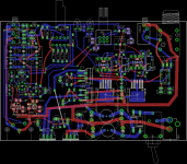
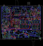
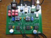
qusp - all good points, thanks. The foil area and/or heatsinks are definitely going to be upgraded. Below is another iteration that I discarded along the way. This one had two LME49600's in parallel on each channel, One OPA827 wrapped around each as a unity gain buffer with 1R balancing resistors on the buffer output similar to the O2 amp. There was a solder-down TO263 ohmite heatsink over each buffer. The bottom set of buffers were on the top of the board, while the top set were on the bottom, both with lots of via holes to transfer the heat.
This amp's LME49600's will probably wind up closer to looking like those bottom two with heatsinks for each. I tossed this design because I couldn't justify the need for two parallel LME49600s per channel for the majority of headphones. How about that for a change? I was the one all eager for parallel buffers on the Wire way back when.
I agree the small OPA827 pad in the middle of the DIP is a bad idea. I've already decided against that one. Instead I will probably just lay down a single SOIC8 pad given that both the OPA627 and OPA827 come in that package. Would save some space over the DIP8 anyway and really is not all that hard to solder. Speaking of hard to solder, I was considering TPS7A30 and TPS7A49 for the small voltage regulators, but those are the smaller package *with a power pad*. Aarrgghh. Not going to happen.
xnor - thanks!
BuildMeSomething - very interesting about the LME49600! Good to know.
abraxalito - really good thought. I agree, in my mind anyway the point of the two separate voltage regulator banks would be to help isolate the low signal chips from the current transients of the buffers. It might make more sense to put both the OPA827 and the gain stage chip on the small voltage regulators if I'm going to use those. Good stuff.
And some more likely changes...
* Add the option to build it up for +/-18Vdc rails instead of +/-16Vdc. I've noticed that both the OPA827 and LME49600 are data sheet qualified for +/-18Vdc operating voltage, with +/-20Vdc maximum. The OPA627 and LME49720HA are only maximum +/-16Vdc though. So to make it work at +/-18Vdc just use 827, 49600, and I would have to come up with a TO99 gain chip good for +/-18Vdc. So far no ideas. The LME49860 is good for +/-20Vdc operating but doesn't come in TO99.
* Might add a variable damping switch after learning about this: Product: HA-501 | TEAC . I've been suspicious for awhile if the low output impedance / high damping factor arangement on amps really produces the best sound on all headphones. Especially after getting a very vague answer back from AKG once about preferred amp output impedance. This would just be another 4 position rotary switch that adds resistance in series with the output on each channel (with one position still 1x/OR of course). I know that RocketScientist cited listening studies about low impedance amps, but this one would just be fun to mess around with, especially since the low impedance 1x position is still there.
qusp - all good points, thanks. The foil area and/or heatsinks are definitely going to be upgraded. Below is another iteration that I discarded along the way. This one had two LME49600's in parallel on each channel, One OPA827 wrapped around each as a unity gain buffer with 1R balancing resistors on the buffer output similar to the O2 amp. There was a solder-down TO263 ohmite heatsink over each buffer. The bottom set of buffers were on the top of the board, while the top set were on the bottom, both with lots of via holes to transfer the heat.
This amp's LME49600's will probably wind up closer to looking like those bottom two with heatsinks for each. I tossed this design because I couldn't justify the need for two parallel LME49600s per channel for the majority of headphones. How about that for a change? I was the one all eager for parallel buffers on the Wire way back when.
I agree the small OPA827 pad in the middle of the DIP is a bad idea. I've already decided against that one.
Instead I will probably just lay down a single SOIC8 pad given that both the OPA627 and OPA827 come in that package. Would save some space over the DIP8 anyway and really is not all that hard to solder. Speaking of hard to solder, I was considering TPS7A30 and TPS7A49 for the small voltage regulators, but those are the smaller package *with a power pad*. Aarrgghh. Not going to happen.xnor - thanks!
BuildMeSomething - very interesting about the LME49600! Good to know.
abraxalito - really good thought. I agree, in my mind anyway the point of the two separate voltage regulator banks would be to help isolate the low signal chips from the current transients of the buffers. It might make more sense to put both the OPA827 and the gain stage chip on the small voltage regulators if I'm going to use those. Good stuff.
And some more likely changes...
* Add the option to build it up for +/-18Vdc rails instead of +/-16Vdc. I've noticed that both the OPA827 and LME49600 are data sheet qualified for +/-18Vdc operating voltage, with +/-20Vdc maximum. The OPA627 and LME49720HA are only maximum +/-16Vdc though. So to make it work at +/-18Vdc just use 827, 49600, and I would have to come up with a TO99 gain chip good for +/-18Vdc. So far no ideas. The LME49860 is good for +/-20Vdc operating but doesn't come in TO99.
* Might add a variable damping switch after learning about this: Product: HA-501 | TEAC . I've been suspicious for awhile if the low output impedance / high damping factor arangement on amps really produces the best sound on all headphones. Especially after getting a very vague answer back from AKG once about preferred amp output impedance. This would just be another 4 position rotary switch that adds resistance in series with the output on each channel (with one position still 1x/OR of course). I know that RocketScientist cited listening studies about low impedance amps, but this one would just be fun to mess around with, especially since the low impedance 1x position is still there.
Attachments
V 4.0 or whatever my ODA project here is up to.
New stuff:
New stuff:
- · Paralleled NJM4556A’s in SIP packages are back with a vengeance. Whether any headphones out there need it or not, 6 op amps per channel now should push about 450mA per channel, which also makes this amp useful for powering small PC speakers. BuildMeSomething’s comment above made me find note #3 on the LME49600 data sheet, and sure enough the THD figures are *with a LME49710* wrapped around it. Which means the inherent THD of the LME49600 (not in an op amp loop) may not be all that much better than an NJM4556. Which means that if I wrap a low(er)-distortion chip like the Wire’s LME49990 running at 1x gain around a bunch of NJM4556A buffers in parallel there is a reasonable shot and linearizing them the same way to some extent. I also missed the economics. The LME49990 is only$2.60 these days, well within RocketScientist/NwAvGuy price range. The LME49600 needs both a chip wrapped around it, more cost, and a heatsink due to the TO-263 package. I see that a TI engineer also recommends 0.1R balancing resistors for parallel operation on their forum (LME49610), which is yet more cost. The NJM4556A SIP plus resistors is about $2 total each. In the spirit of Rocket Scientist’s O2 amp, cheap cheap cheap!
- · Back to just one set of regulators star’ed off a central point, the low noise LT1963A abd LT3015 heatsinked to the case. I agree with qusp’s comment, proper bypassing at the device level (nearby) will likely do boatloads more than additional regulators. Associated with this change, more decoupling caps added.
- · The simple BD139 circuit added to the positive regulator input to knock 3V off the incoming voltage and stay within the chip’s 20Vdc input. Recall that zener diodes of 3.6V or less are all mostly zener breakdown, relatively quiet, and those above 3.6V are avalanche breakdown and 10x noisier. Probably no significant noise benefit here to using a white LED vs. the 3.6v zener, especially since the LT regulator is supposed to clean it up.
- · Adjustable system voltage! This may be something new in headphone amps. Something else that I tried talking RocketScientist into considering for the ODA. Since the volatage regulators are adjustable it is easy to add a 3 position switch changing one resistor. +/-8Vdc rails for IEMS and PC speakers, +/-12Vdc rails same as the O2 for phones and PC speakers, and +/-16Vdc for 300 ohm and 600 ohm headphones. The switch is mounted off the PC board above the voltage regulators on the case back panel. Otherwise just stick a resistor in the two holes for one single system voltage. The benefit here is reduced chip dissipation for loads that don’t need high voltage. The downside is potentially a bit higher distortion at the lower system voltage, although +/-8Vdc is still a ways above the chip minimum of 2.5Vdc. If the voltage is set too low the result will be clipping, but now there is a clipping indicator so no big deal.
- · I’m keeping the LME49720HA gain chip, even though a lower distortion rated LME49990 is wrapped around the NJM4556 buffers on each channel now, since I still suspect the resulting distortion levels of the buffer chips will be above even the LME49720, making a lower distortion chip a waste of money. Cheap cheap cheap, as per RocketScientist’s philosophy! J The LME49720HA is twice the cost of a LME49990, but it would take two LME49990 and just one (dual) LME49720HA.
- · The front panel ¼ inch jack and rear RCA jacks are now gone from the PC board, but will fit just fine mounted to the case front and back panels above the output jack and regulator, respectively. This is done to shrink it back down to a 80x100 PC board, the size in the O2 amp, which is the cheapest to fab. I can get 80x100mm for $2.50 each (set of 10 for $25) plus shipping at iTEADstudio or Seeed studio in China. A 80x125mm that fits in the B5-080 case jumps up to $10 (5 for $50). As per RocketScientist’s philosophy, cheap cheap cheap!
- · The case is now the B3-080, the taller version of the O2's B2-080 case, which is also relatively cheap. $5 less than the B5-080 case anyway. The B3 cases are also much more available, with the various distributors having many in stock. The B5 cases are scarce.
- · Related to the PCB and case change above, something slick can now be done to add an ODAC inside the amp. Just get the stretch B3-160 case and use 2 of these PC boards. Only populate the power supply parts for the one in back and mount the ODAC on the unused space in front. Then on the front PC board populate everything but the power supply parts and just cable power over from the back board to the front board.
- · Diode snubbers ala Hagerman are back (thanks transistormarkj for the suggestion)
- · Bigger filter caps. I forgot to use 50V units before to handle higher voltage AC adaptors. 12.5mm units now instead of 10mm.
- · Clipping detect circuit added! Connects to the output of the gain stage and flashes a LED when the output gets near the rails via a window comparator. Circuit isn’t mine – from the net – but does the job. I’ve used a TLO64 for the “comparator” since I don’t need extreme speed for this and don’t want to use pulldown resistors. The TL064 has a slew rate rating that can handle the full voltage output swing of the first stage.
- · Relay control circuit added, along with a 5V regulator. The circuit produces the 2 second turn on delay before the relay connects the headphones. The 5v regulator allows a 5V relay to be used regardless of the (now variable) rail voltages.
- · I’ve started a BOM which I’ll post out on Google Docs like RocketScientist did for the O2. Looks like the parts cost with case will be around $100. But that is not including the 6 input DC blocking caps I’ve added. Those Wima things are $2.5 each, so would add $15 just for the caps. Not required (just bypass them to save the money), the blocking cap from the O2 is still in the center and the clipping indicator is added now, but recommended.
- · 4 position gain rotary switch remains, along with 1x.
Attachments
Last edited:
I think that I'm getting close to sending the board in for fab. Still have been messing around with a few things. With any luck I'll have it out to fab early next week.
I have high resolution PDF versions of the layout and circuit (same as the png's below but high rez) on Google Docs at:
https://drive.google.com/folderview?id=0B67cJELZW-i8VmhVNk5PODNtZnc&usp=sharing
click on each image to bring up the PDF in a viewer, or hit the Google download button to download the PDF.
New stuff:
Still have been messing around with a few things. With any luck I'll have it out to fab early next week.I have high resolution PDF versions of the layout and circuit (same as the png's below but high rez) on Google Docs at:
https://drive.google.com/folderview?id=0B67cJELZW-i8VmhVNk5PODNtZnc&usp=sharing
click on each image to bring up the PDF in a viewer, or hit the Google download button to download the PDF.
New stuff:
- · Highest power rail voltage switch setting now +/-17Vdc since all the chips have up to +/-18Vdc operating voltage (+/-20Vdc max), and I find that the LME49720 and LLME49990 are fully specified at +/-17V rails in their datasheet graphs (the LME49990 at +/-18Vdc). The mid voltage setting is still +/-12 and the low is now +/-7Vdc. +/-17Vdc translates to about 14V peak swing, which is about 10Vrms. That is 14V – 7V = 7V more peak swing than the O2 amplifier for those hard-to-drive 600 ohm low sensitivity cans.
- · I found a slick change that actually justifies both the LME49720 (over the NJM2068 in the O2 amp) and the heatsink ability of the T0-99 HA metal can version. The pot and attenuation resistor (still in the middle like the O2) are now 1K to reduce Johnson/thermal noise, since I discovered the LME49720 is fully specified at 600 ohms output load (at +/-17Vdc rails, too). The 40.2K input bias current ground return resistor in the O2 amp and feedback resistor for the NJM4556As is subsequently reduced to 10K for Johnson/thermal noise reduction, still large enough not to have a taper-alterning effect on the pot. That would be 7mA peak through the LME49720 output section (and pot + resistor) at 17Vdc rails (14Vdc max swing), well within the 23mA output maximum for the part. The NJM2068 only appears to be specified down to 2k loads, while the LME49720 is specified in the data sheet for both 2k and 600 ohm loads, so this is a potential noise improvement over the O2 amp. The TO-99 metal can part is heat-sinkable too, which I've now provided space for on the layout. The higher current draw fits right in with a desktop amp but would be a non-starter for a portable amp like the O2, which is probably why RocketScientist/NwAvGuy never did this in the O2. The LME49990 input bias ground return resistors could actually be dropped 10x to 4.02K, but that would require another capacitor that won't fit to maintain the corner frequency. As it sits I've beefed up the middle coupling cap to 2x 4.7uF to maintain Fc with the 10k resistors same as RocketScientist's O2.
- Two hiccups related to the above 1K pot. Right now Mouser only has linear taper 1K 9mm Bourns pots in stock, with the audio taper on order for delivery in a month. The other is that the linear 9mm pot has a maximum power dissipation of just 50mW and the audio of 25mW. So the 1k pot must be used with the 50/50 attenuation resistor (1K resistor in this case) which cuts the maximum swing in half. That drops the pot maximum power dissipation to 16mW. If the full 14V swing is needed use the regular 10K pot instead with no attenuation resistor. However, that is worst case 14V peak sine wave = 10Vrms sine wave. When "music power" is taken into account the average power in the pot would easily be 1/2 that, and more likely 1/3, so the 1K pot with no attenuation resistor would still likely be OK if someone wants to play the averages.
- · SMD pads added for X2Y EMI suppression 1206 caps added at the input jack, output jack, and power supply jack as a test to try nuking cell phone EMI, as per the recent posts in this thread: http://www.diyaudio.com/forums/headphone-systems/233023-rfi-problems-diy-headphone-amp.html . These are optional, of course. There have been several posts about cell phone radiation affecting the O2 amp.
- · Bass boost is back. I've added holes for the resistor and capacitor in the mod I posted, along with holes to run wires out to an external DPST switch mounted on the front panel. Boost is optional - the two resistors and caps can simply be left off.
- · I've been messing around with laying out the circuit on the 80mm x 160mm PCB to fit the B5-080 and B5-160 case. Turns out the B5 cases are readily available at the distributors, unlike the B4 cases. The B5-080 case is the same depth as the O2 B2-080 case, but 2.4 inches wider and 3/4 inch taller. Essentially the same circuit with the layout tweeked a bit to add the front panel 1/4 inch jack and rear RCA jacks back. Plus space for extra stuff like the voltage control knob in back and damping factor switch in front. The B5 PCB is a lot more expensive through, about $20 each from iTeadstudio (5 for $100). Really too expensive to be RocketScientist friendly, I would think. But the layout tweaks are easy so I'll post the gerbers for that anyway once it is all tested. For this layout the 1/4 inch jack and RCA jacks still fits, mounted to the front panel or an upper PCB in the upper B3-080 slot
- Another benefit of the smaller and cheaper 80mm x 100mm board is that 4 layer becomes affordable (center ground plane). The 4 layer 80 x 100 is $20 per board (5 for $100) again, also not a RocketScientist friendly number, but probably would provide a noise floor improvement.
- DC servo. The OPA627 andOPA827 are gone but not forgotten. The goal I was after with those was a very small DC output offset on the amp output. The OPA627 in particular has the exceptionally low input offset voltage and low input bias current. Well I've recently discovered the OPA2188 / OPA188 while look ideal for a DC servo and are low cost at just $3 for the dual. Even lower output offset voltage than the 627 - just 25uV max - since they are choppers. BUT, unlike most choppers, these appear to have a notch filter on-board at the chop frequency so one isn't apparently needed on the output. And they have input bias current in the 100's of pico-amps. There is no room on the 80 x 100 PCB for servos but I will probably add it to the 80 x 160 layout, along with the 3 pole input LPF on each that I posted in the DIYA wiki section.
- Related to the above, I ordered some SOIC8 to DIP8 adaptors, soldered on a couple of LME49990s, and stuffed them into the PCB at the top of this thread that has the 2 paralleled NJM4556A sections on each channel (4x op amps in parallel on each channel). Works great! Photo below. This would be the same configuration as this new PC board when running at 1x gain, but this new board has 6x op amps per channel. In fact I listened to it for nearly two hours while doing some computer work. The LME49990 + parallel NJM4556A (subjectively) rocks!
Attachments
Last edited:
typos and gain chip change to LM49990s
I had a chance to read the LME49990 datasheet in more detail this afternoon. I came to realize it is also rated for a 600 ohm load, same as the LME49720. But the THD graph of the LME49720 vs. output voltage swing has an inflection point at around 4V, then the THD starts going up again. The LME49990 has no such problem, with progressively decreasing distortion all the way to a 10V swing on 18Vdc rails.
So given that the LME49990 is priced at just $2.60 these days vs. $7 for the LME49720 part, I've thrown in the towel on the LME49720 and switched to two LME49990s for the gain stage. Just left with absolutely nothing to justify the price of the LME49720 part vs. the O2's $0.70 NJM2068 or the better-spec'ed LME49990s for $5 for the pair. RocketScientist/NwAvGuy never did evaluate the LME49990, but at the time the chip was around $10 each as I recall, out of the "cheap" category. If he were doing the reviews today I'll bet he would take a hard look at the LME49990 for the O2.
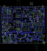
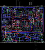
At any rate the new layout is attached below. The chips are side by side, one of the top of the board and one on the bottom, with the 0.22uF EPCOS film caps from the O2 on the rails for bypass.
I typo'ed the alternate box size in the post above. The B4-080 and B4-160 cases are the larger ones that are widely available. The B5-080 case is the one that is less wide, less tall, and rather scarce.
And I forgot to mention why +/-7Vdc is the low rail selection voltage. That is the voltage that the O2's power management circuit cuts off if running on batteries. Seemed like a fitting voltage to use. The middle voltage is +/-12Vdc since that is the O2's AC voltage of course, and the +/-17Vdc high voltage is as described.
The question will probably come up "why not just power 600R headphones directly like a CMOY from the LME49990 if it can handle 600 ohm loads?" The answer is capacitance, that is 600R resistive. The chip is rated for about 100pF on the output, more than typical headphone cable. That is also why I've included the 20R resistor on the output of each LME49990 powering the 3 NJM4556AL chips, given the capacitance of the chip inputs and the trace lengths involved in stringing together the chips inputs.
It also looks like the maximum usable swing from the chips will be around +/-10.5Vdc with the +/-17Vdc rails, not +/-14Vdc as I estimated above. The chip overhead into a 2K load is higher than I expected. That is still substantially more swing than the O2 for high impedance cans though.
I also forgot to say that in the case of the OPA2188 and a DC servo, the very slow slew rate of the part shouldn't matter given the 3 pole low pass filter on the input of the integrator. Even with a 10.5V output swing on the amplifier at 10Hz, after the filter there just isn't that much voltage swing left to slew. Getting close to DC.
I had a chance to read the LME49990 datasheet in more detail this afternoon. I came to realize it is also rated for a 600 ohm load, same as the LME49720. But the THD graph of the LME49720 vs. output voltage swing has an inflection point at around 4V, then the THD starts going up again. The LME49990 has no such problem, with progressively decreasing distortion all the way to a 10V swing on 18Vdc rails.
So given that the LME49990 is priced at just $2.60 these days vs. $7 for the LME49720 part, I've thrown in the towel on the LME49720 and switched to two LME49990s for the gain stage. Just left with absolutely nothing to justify the price of the LME49720 part vs. the O2's $0.70 NJM2068 or the better-spec'ed LME49990s for $5 for the pair. RocketScientist/NwAvGuy never did evaluate the LME49990, but at the time the chip was around $10 each as I recall, out of the "cheap" category. If he were doing the reviews today I'll bet he would take a hard look at the LME49990 for the O2.
At any rate the new layout is attached below. The chips are side by side, one of the top of the board and one on the bottom, with the 0.22uF EPCOS film caps from the O2 on the rails for bypass.
I typo'ed the alternate box size in the post above. The B4-080 and B4-160 cases are the larger ones that are widely available. The B5-080 case is the one that is less wide, less tall, and rather scarce.
And I forgot to mention why +/-7Vdc is the low rail selection voltage. That is the voltage that the O2's power management circuit cuts off if running on batteries. Seemed like a fitting voltage to use. The middle voltage is +/-12Vdc since that is the O2's AC voltage of course, and the +/-17Vdc high voltage is as described.
The question will probably come up "why not just power 600R headphones directly like a CMOY from the LME49990 if it can handle 600 ohm loads?" The answer is capacitance, that is 600R resistive. The chip is rated for about 100pF on the output, more than typical headphone cable. That is also why I've included the 20R resistor on the output of each LME49990 powering the 3 NJM4556AL chips, given the capacitance of the chip inputs and the trace lengths involved in stringing together the chips inputs.
It also looks like the maximum usable swing from the chips will be around +/-10.5Vdc with the +/-17Vdc rails, not +/-14Vdc as I estimated above. The chip overhead into a 2K load is higher than I expected. That is still substantially more swing than the O2 for high impedance cans though.
I also forgot to say that in the case of the OPA2188 and a DC servo, the very slow slew rate of the part shouldn't matter given the 3 pole low pass filter on the input of the integrator. Even with a 10.5V output swing on the amplifier at 10Hz, after the filter there just isn't that much voltage swing left to slew. Getting close to DC.
Attachments
Last edited:
Good! Glad to know things are moving in right direction on the O2 desktop front.
I'll be interested to hear the results myself!
The latest stuff is at the Google link in the post above in the 4/8/2013 folder, including a first pass at a BOM. Looks like about $120 for parts and another $25 for case / power adaptor / PCB. I've attached a summary below of the differences between this version of an ODA and RocketScientist/NwAvGuy's O2 headphone amp.
I just keep messing with it.
Latest stuff for the 80x100mm (O2 sized) version in the B3-080 case:* Two NJM4556AL buffers per channel now down from 3 to allow proper airflow (cooling) around the chips. Power supply re-sized to match.
* I was able to fit a DC servo using the OPA188 on one channel as a test of the circuit. The servo parts don't have to be populated - optional. The bigger version on a 80 x 160mm PCB in the B4-080 case will have servos on both channels and back to 3 NJM4556AL chips per channel.
* Input coupling caps are gone and instead the O2-style coupling capacitor in the middle is increased to 3x 4.7uF on each channel to drop the corner frequency to 1.3Hz. The O2 is 1.8Hz.
* Clipping detect LED now by the input jack and volume control.
* Optional SMD bypass caps added right at each NJM4556AL buffer chip's power pins. I haven't had any oscillation problems at all with the test PCB I'm using with the LME49990 wrapped around two NJM4556A's, but the pads are there just in case.
I'll be curious to see if I can eventually get this amp to measure at least slightly better than the O2 in a few areas. I'm up to the challenge.
Attachments
Last edited:
I'am sure you will.....I'll be curious to see if I can eventually get this amp to measure at least slightly better than the O2 in a few areas. I'm up to the challenge.
Best of luck
The design just did another morph. I had actually sent it out for fab a couple of days ago but immediately had regrets over not having a 1/4" output jack and RCA input jack mounted on the PCB. Thinking about it some more those two seem like requirements for a desktop headphone amp. Plus I remember RocketScientist / NwAvGuy posting in a comment somewhere that he was going to have a 1/4" jack on his ODA. So I've cancelled the order and went back at it.
New stuff is at the Google docs link in the post above and a summary below. The PCB is now the more pricey ($14) 80mm x 160mm size that fits the more pricey ($18.50) B4-080 aluminum case that is 2.5 inches wider and 1 inch taller than the O2. 3 buffers per channel again, DC servos on both channels, pre-regulators again, and other good stuff.
I had actually sent it out for fab a couple of days ago but immediately had regrets over not having a 1/4" output jack and RCA input jack mounted on the PCB. Thinking about it some more those two seem like requirements for a desktop headphone amp. Plus I remember RocketScientist / NwAvGuy posting in a comment somewhere that he was going to have a 1/4" jack on his ODA. So I've cancelled the order and went back at it. New stuff is at the Google docs link in the post above and a summary below. The PCB is now the more pricey ($14) 80mm x 160mm size that fits the more pricey ($18.50) B4-080 aluminum case that is 2.5 inches wider and 1 inch taller than the O2. 3 buffers per channel again, DC servos on both channels, pre-regulators again, and other good stuff.
Attachments
Last edited:
I've been closely watching your progress and thought I'd my 2 cents.
I have an O2 setup as a desktop amp. I added a switch and some RCA outs to use it as a pre-amp for my Honey Badger. There's an open spot next to your 3.5mm that would be a good spot for an optional switch. Maybe by default, the 3.5mm and 1/4" are parallel. How about an option for manually switching them? I would exclude the 3.5mm and switch between RCA out and 1/4" out. With your current layout (1/4" on the board), I would have to cut the parallel traces to switch off the headphones. Yes, I am too lazy to unplug them.
I have an O2 setup as a desktop amp. I added a switch and some RCA outs to use it as a pre-amp for my Honey Badger. There's an open spot next to your 3.5mm that would be a good spot for an optional switch. Maybe by default, the 3.5mm and 1/4" are parallel. How about an option for manually switching them? I would exclude the 3.5mm and switch between RCA out and 1/4" out. With your current layout (1/4" on the board), I would have to cut the parallel traces to switch off the headphones. Yes, I am too lazy to unplug them.
Lukky - good thoughts, I've been thinking about a pre-amp out. I know a that a lot of folks have asked for that in the O2 amp thread here and over in the comments on RocketScientist / NwAvGuy's blog. So far I've been planning on handling pre-amp outs with externally mounted parts. The extra inch of height in that B4-080 box over the O2' s B2-080 case for add-ons and modificationsis is another thing that led me to go that route.
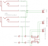
I think I have a good solution for what you are after. Those two resistors to the left of the 3.5mm output jack, R61 and R62, are new (vs. the O2). They are ostensibly for adding optional series resistance between the relay and output jacks to change the damping factor. But they can also just be jumpered with a wire and the output of the buffer chips run right to the output jacks, as in the O2.
But in your case your could mount a panel-mount DPDT switch and panel mount RCA jacks in the inch or so above those 3.5 and 1/4" output jacks. Then wire it up with a DPDT switch as the first attachment below, with R61 and R62 left off the board, and instead wires go from those holes to the DPDT switch as shown. In one switch position the relay output goes to the jacks and in the other the jacks are cut off and the output goes to your RCA pre-amp out jacks.
But... an idea just hit me. I really should add PCB holes for connecting wires to the output of the gain stage itself, right at the outputs of the gain stage LME49990 chips (the inputs to the pot in the middle). That way pre-amp out could be taken off right from the gain stage, a more appropriate place, with no need to plow through that 1x output current buffer stage. Also isolates the pre-amp outs from the headphone outs.
The LME49990 is fully specified with a 600 ohm load. In fact the AC number gets slightly better at 600R than 2K from the datasheet graphs. So if you are using the new 1K (lower noise) pot option in the ODA, then attach a 10K input to your amp at those pre-amp outs, that is still just 1K || 10K = 900 ohms, well within load range for the gain stage. You could even drop an amp input all the way down to 1.5K on those pre-amp outputs and still be at 600R total load on the gain stage with the 1K pot.
So instead you could wire things up as the second attachment below. Use a 4PDT panel mount toggle switch like #633-M204205 at Mouser
M2042LL1W01 NKK Switches | Mouser
and wire it up with using wires from those new gain stage out holes on the PCB. In one position the gain stage out is routed to your pre-amp outs and the jacks are cut off via wires from those R61 R62 holes to the other half of the switch. Then in the other position your pre-amp outs are cut off and the headphone jacks are on. Or, just connect the gain stage output wires directly to the pre-amp out RCAs to have those on all the time, but put a DPDT on the jacks via the method above with the R61 R62 holes to switch the headphones off.
Lots of options! The RCA pre-amp output jacks could be mounted on the back panel too. I like to facilitate modifications, even on my own designs!
Click on the arrows in the lower left corner of the pix below, once they are open, to blow them up to readable size.
I think I have a good solution for what you are after. Those two resistors to the left of the 3.5mm output jack, R61 and R62, are new (vs. the O2). They are ostensibly for adding optional series resistance between the relay and output jacks to change the damping factor. But they can also just be jumpered with a wire and the output of the buffer chips run right to the output jacks, as in the O2.
But in your case your could mount a panel-mount DPDT switch and panel mount RCA jacks in the inch or so above those 3.5 and 1/4" output jacks. Then wire it up with a DPDT switch as the first attachment below, with R61 and R62 left off the board, and instead wires go from those holes to the DPDT switch as shown. In one switch position the relay output goes to the jacks and in the other the jacks are cut off and the output goes to your RCA pre-amp out jacks.
But... an idea just hit me.
I really should add PCB holes for connecting wires to the output of the gain stage itself, right at the outputs of the gain stage LME49990 chips (the inputs to the pot in the middle). That way pre-amp out could be taken off right from the gain stage, a more appropriate place, with no need to plow through that 1x output current buffer stage. Also isolates the pre-amp outs from the headphone outs.The LME49990 is fully specified with a 600 ohm load. In fact the AC number gets slightly better at 600R than 2K from the datasheet graphs. So if you are using the new 1K (lower noise) pot option in the ODA, then attach a 10K input to your amp at those pre-amp outs, that is still just 1K || 10K = 900 ohms, well within load range for the gain stage. You could even drop an amp input all the way down to 1.5K on those pre-amp outputs and still be at 600R total load on the gain stage with the 1K pot.
So instead you could wire things up as the second attachment below. Use a 4PDT panel mount toggle switch like #633-M204205 at Mouser
M2042LL1W01 NKK Switches | Mouser
and wire it up with using wires from those new gain stage out holes on the PCB. In one position the gain stage out is routed to your pre-amp outs and the jacks are cut off via wires from those R61 R62 holes to the other half of the switch. Then in the other position your pre-amp outs are cut off and the headphone jacks are on. Or, just connect the gain stage output wires directly to the pre-amp out RCAs to have those on all the time, but put a DPDT on the jacks via the method above with the R61 R62 holes to switch the headphones off.
Lots of options! The RCA pre-amp output jacks could be mounted on the back panel too. I like to facilitate modifications, even on my own designs!
Click on the arrows in the lower left corner of the pix below, once they are open, to blow them up to readable size.
Attachments
Last edited:
uncola - I agree, I think it looks kind of bad having the power jack on the front. NwAvGuy probably did that in part to keep costs down, so that only one custom drilled panel would be needed. For the desktop unit though the power really should come in via the back, I think.
The power switch would probably be handier in front, but electrically and from a layout standpoint having the switch in back won. I wanted the switch right on the AC lines to fully cut off everything when off (and easier on switch contacts to "break" AC than DC), unlike the O2 that left the AC power supply running regardless. So if the switch wasn't in back I would have to run noisy AC lines through the PCB, or add a relay. Easiest to just have it in back.
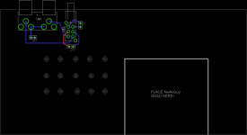
I've left space in this one for RocketScientist / NwAvGuy's ODAC. Another plus on using the taller box. I've made sure none of the parts stick up so far as to prevent a second PCB being slid into the top slot in the box, upside down so the parts hang down and the solder joints face up. I've been thinking about whipping up an "accessory board" like that with a full Baxendall tone control, crossfeed, etc., and the space for an ODAC. That upper board doesn't necessary have to be an etched PCB for just mounting the ODAC. A piece of 160mm wide perf-board, or even copper clad board, from the local Radio Shack or other hobby store would work just fine for mounting the ODAC in the top slot. If the ODAC is butted up against the back panel a mini-USB slot could be cut into the back panel along with the other holes. The ODA PCB has holes near the input jack for hooking in the ODAC output or any other connection to the signal input lines.
There is also a B4-160 case available (twice as long) which is another way to do it. Two of these PCBs could be used end to end like I was going to do with the 80x100 PCB. Only the power supply parts can be populated on the back one, an ODAC mounted on the front 2/3, then the power cabled over to the front board that doesn't have the PS parts popluated. I've added PCB holes on the power supply lines to allow cabling like that, or to tap off power for an accessory board on the top.
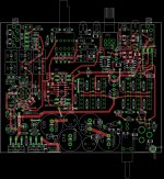
I just whipped up an example layout below that has Lukky's idea for the RCA pre-amp outs (horizontal jack in this case instead of the vertical input jack on the main ODA board) and a switch. Plus the area for an ODAC and holes to let the heat from the buffer chips make it on up to the top of the aluminum case.
The power switch would probably be handier in front, but electrically and from a layout standpoint having the switch in back won. I wanted the switch right on the AC lines to fully cut off everything when off (and easier on switch contacts to "break" AC than DC), unlike the O2 that left the AC power supply running regardless. So if the switch wasn't in back I would have to run noisy AC lines through the PCB, or add a relay. Easiest to just have it in back.
I've left space in this one for RocketScientist / NwAvGuy's ODAC.
Another plus on using the taller box. I've made sure none of the parts stick up so far as to prevent a second PCB being slid into the top slot in the box, upside down so the parts hang down and the solder joints face up. I've been thinking about whipping up an "accessory board" like that with a full Baxendall tone control, crossfeed, etc., and the space for an ODAC. That upper board doesn't necessary have to be an etched PCB for just mounting the ODAC. A piece of 160mm wide perf-board, or even copper clad board, from the local Radio Shack or other hobby store would work just fine for mounting the ODAC in the top slot. If the ODAC is butted up against the back panel a mini-USB slot could be cut into the back panel along with the other holes. The ODA PCB has holes near the input jack for hooking in the ODAC output or any other connection to the signal input lines.There is also a B4-160 case available (twice as long) which is another way to do it. Two of these PCBs could be used end to end like I was going to do with the 80x100 PCB. Only the power supply parts can be populated on the back one, an ODAC mounted on the front 2/3, then the power cabled over to the front board that doesn't have the PS parts popluated. I've added PCB holes on the power supply lines to allow cabling like that, or to tap off power for an accessory board on the top.
I just whipped up an example layout below that has Lukky's idea for the RCA pre-amp outs (horizontal jack in this case instead of the vertical input jack on the main ODA board) and a switch. Plus the area for an ODAC and holes to let the heat from the buffer chips make it on up to the top of the aluminum case.
Attachments
Last edited:
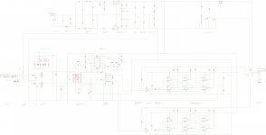
differential drive - moar powerz! - and gain stage bypass
Here are two more somewhat slick things that can be done with this version of an ODA:
* Differential drive to double the output swing to +/-20Vdc.
The two channels of a single ODA can be differentially driven for extremely hard-to-drive high impedance headphones by a chip like the OPA1632 that opc used in the balanced Wire amp. The two wires for one headphone channel hook to the signal out on each channel and effectively receive twice the voltage swing, about +/-20V. The OPA1632 can be mounted on a top-slot accessory board, as mentioned in the post above.
Note that two ODA's would be needed, one for each channel, since the two channels in each one form the differential drive for each headphone channel.
Doing differential drive is nothing new and has been mentioned a lot on the forum. What is new is that now the buffer chips can handle the dissipation. That has been in the back of my mind in beefing up the number of parallel output chips. The load looks like half the impedance in bridged mode and usually winds up overheating the output chips. That would be the likely outcome of the O2 run in bridged mode. The ODA here has no such problem. Since the headphones are assumed to be high impedance (600R etc) the current requirements will be relatively low and the buffer chips should be sufficient to dissipate that much voltage swing.
The other thing that is new is that with two ODAs, each is run off a separate AC wall wart, which means the power supplies are isolated from each other. The other thing that can happen in bridged mode is the common ground wire in the headphone cable winds up shorting out the amp unless the headphone cable is restrung to have two separate wires to each driver. Here that shouldn't be a problem since the two ODAs, one for each earcup, are isolated at the wall wart.
* Gain stage bypassing. In addition to PCB holes at the output of the gain stage chip I've added O ohm jumper resistors before those, between the gain stage chip and the tap off. So now if the OR resistors are left off the gain stage chips and parts can be left unpopulated and the amplifier input after the RF filter run directly to the 1K or 10K pot (and series attenuation resistors if they are installed) and on to the output current buffer stage. That arrangement is for people who don't need any voltage gain due to higher voltage sources but still need current buffering.
Here are two more somewhat slick things that can be done with this version of an ODA:
* Differential drive to double the output swing to +/-20Vdc.
The two channels of a single ODA can be differentially driven for extremely hard-to-drive high impedance headphones by a chip like the OPA1632 that opc used in the balanced Wire amp. The two wires for one headphone channel hook to the signal out on each channel and effectively receive twice the voltage swing, about +/-20V. The OPA1632 can be mounted on a top-slot accessory board, as mentioned in the post above.
Note that two ODA's would be needed, one for each channel, since the two channels in each one form the differential drive for each headphone channel.
Doing differential drive is nothing new and has been mentioned a lot on the forum. What is new is that now the buffer chips can handle the dissipation.
That has been in the back of my mind in beefing up the number of parallel output chips. The load looks like half the impedance in bridged mode and usually winds up overheating the output chips. That would be the likely outcome of the O2 run in bridged mode. The ODA here has no such problem. Since the headphones are assumed to be high impedance (600R etc) the current requirements will be relatively low and the buffer chips should be sufficient to dissipate that much voltage swing.The other thing that is new is that with two ODAs, each is run off a separate AC wall wart, which means the power supplies are isolated from each other. The other thing that can happen in bridged mode is the common ground wire in the headphone cable winds up shorting out the amp unless the headphone cable is restrung to have two separate wires to each driver. Here that shouldn't be a problem since the two ODAs, one for each earcup, are isolated at the wall wart.
* Gain stage bypassing. In addition to PCB holes at the output of the gain stage chip I've added O ohm jumper resistors before those, between the gain stage chip and the tap off. So now if the OR resistors are left off the gain stage chips and parts can be left unpopulated and the amplifier input after the RF filter run directly to the 1K or 10K pot (and series attenuation resistors if they are installed) and on to the output current buffer stage. That arrangement is for people who don't need any voltage gain due to higher voltage sources but still need current buffering.
Last edited:
- Home
- Amplifiers
- Headphone Systems
- A version of an O2 Desktop Amp (ODA)