Note on the prototype build
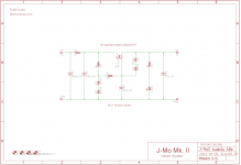
I'll be using the J202 and the circuit will be changed a fair bit to make it optimized for my 300 ohm HD-600 headphones. I will also substitute the 2SK213 for the IRF510. I mean, it's available at my local marutsu there's really no excuse not to.
The J202 works at around 1.2 V bias, and for the HD-600, I need as much voltage as possible, so the input to the mosfet should be [(V++/2) + 2] = 12 V Which means a gain of about 10x. I don't need so much current, so the mosfet source resistor will be increased to 150 ohms.
Attachments
Thanks! Unfortunately those little boards are only half the story: unlike my usual modus operandi the regulators and all that are missing from the main board and have to be dealt with elsewhere.
Though for first run testing I'll just use a benchtop lab supply.
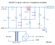
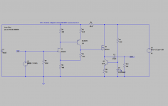
I'm working on developing a Z-reg circuit, tailored to my own high impedance version. It's sufficiently low current that I can use my standard 12x2 VAC transformer and drop the 36 V rectified DC though another IRF510/2SK213 using a pair of 12V Zeners --- all parts I have on hand. Output comes to 20 V, with 0.1 mV ripple. Turn on is 1s soft start, and the mosfet gate is protected from turn-off transients by a Zener stack.
See attached. (still kinda rough) R3 is a placeholder for the real load of the JMO2 circuit itself.
This will work for the regular high current version too, but you are looking at 5W dissipation in the IRF510, so a fairly big (~5 C/W) heatsink. It would probably be more sensible to use a lower secondary voltage of 15 or 16 VAC, a 20 V Zener, and a npn transistor as the pass element.
Though for first run testing I'll just use a benchtop lab supply.
I'm working on developing a Z-reg circuit, tailored to my own high impedance version. It's sufficiently low current that I can use my standard 12x2 VAC transformer and drop the 36 V rectified DC though another IRF510/2SK213 using a pair of 12V Zeners --- all parts I have on hand. Output comes to 20 V, with 0.1 mV ripple. Turn on is 1s soft start, and the mosfet gate is protected from turn-off transients by a Zener stack.
See attached. (still kinda rough) R3 is a placeholder for the real load of the JMO2 circuit itself.
This will work for the regular high current version too, but you are looking at 5W dissipation in the IRF510, so a fairly big (~5 C/W) heatsink. It would probably be more sensible to use a lower secondary voltage of 15 or 16 VAC, a 20 V Zener, and a npn transistor as the pass element.
Attachments
Last edited:
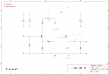
Simulation results:
Voltage gain: 3 (9.5 dB).
Heat: 1W source resistor, 2W MOSFET, 2W Z-reg MOSFET (4W if shared). 10 W for the full stereo circuit.
Max output power before clipping: 100 mW into 16 ohms, 100 mW into 30 ohms, 90 mW into 100 ohms, 40 mW into 300 ohms.
"Nominal" clean power output for 0.1% THD: about 10 mW for 16 and 30 ohms, falling to 1 mW for 300 ohms.
The circuit is optimized for 16-50 ohm headphones, from the standpoint of both output power and gain.
To get better performance with 300 ohm headphones, there are a number of changes that should be made, starting by replacing the 2N5486 with the 2N5485 or J202, increasing the gain to 10, increasing the MOSFET source resistance to 150 ohms, and increasing the power supply to 20-24 V. I will publish the modification later.
Attachments
Simulation results:
Voltage gain: 3 (9.5 dB).
I've found that even 6dB of gain in a headphone amp is too much when directly connected to a typical DAC or CD player, even with a volume pot on the input to the amp. I think the standard is something like 2volts output?
It's an interesting circuit.
The headphone amplifier gain question... answered.
I should probably write this up definitively as a blog post, but I'll sketch it out here first.
Yes, line level audio is 2 V (rms). Many sources, such as phono stages and portable audio, are a fair bit less, as low as 250 mV. As a practical matter, most people would want the volume control at the 9-10 o'clock position for "normal" listening.
How loud the sound is depends on the source signal amplitude, the position of the volume control, the circuit gain, and the impedance and sensitivity of the headphones.
For standard "line level" source, the gain required to keep the volume control at a reasonable setting of 9-10 o'clock varies over 12 dB depending on the impedance of the headphones roughly as follows:
Impedance____Gain
16 ohms______9 dB 3x
32 ohms______12 dB 4x
65 ohms______15 dB 6x
120 ohms_____18 dB 8x
300 ohms_____22 dB 12x
That's "normalized" to the sensitivity of my HD-600's. For IEMs drop the gain down a factor of two.
Short story is if the gain is adjusted to be just right with 16 ohm headphones, you'll have to turn up the volume control way past 12 oclock with 300 ohm headphones. If the gain is just right for 300 ohm headphones, the volume control will be will be barely off -inf, stuck in the non-linear tracking region, with 16 ohm 'phones.
You have four options.
1. Cut your losses. The amp is designed either for high impedance or low impedance headphones, but not both.
2. Take the middle road. Around 5-6x gain 14-15 dB is good enough to be workable with all headphones, but will be increasingly non-ideal at the extremes.
3. Make the switch. Configure the circuit to work at two different gains, with a dip-switch of front panel control to change a feedback resistance or voltage divider network.
4. Linearize. Add a 33-120 ohm in series with the load. The net gain of the circuit automatically self-adjusts depending on the headphone impedance in such a way as the attenuation is greater the lower the impedance.
There are pros and cons to all four. After careful consideration I generally tend to favor method 1, and I am following that here with the J-Mo mk. ii. The version I am making is optimized for my 300 ohm HD600s, while the "official" circuit is tuned for 16-65 ohm loads.
Last edited:
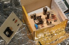
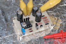
It lives!
I simulated the crap out of this circuit, so it's not so surprising really, but its still a thrill to see everything come together as planned. The MOSFET source bias ends up exactly where the simulation predicted, and can be adjusted 1 V up or down by a about 1 turn of the 14 turn trimmer resistor. The bias is stable and easily matched between channels to 10-20 mV or so.
Things pause for a bit now, there isn't much I can do except build the full amp including the regulators and start listening.
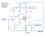
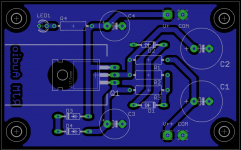
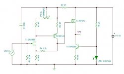
Build details:
Q1 = J202
Q2 = BD140
Q3 = 2SK213
R1, R8 = 75k Welwyn
R2 = 475R||475R = 237.5R Vishay 1/2W
R3 = 4k75 Vishay 1/2W
R4, R6, R9 = 47R Kamaya carbon
R5 = Vishay 1k trim
R7 = 150 ohm 2 W, Vishay PR02
C1,2,3 = Nichicon KZ 100u 50V (yeah, those. I splurged...)
I simulated the crap out of this circuit, so it's not so surprising really, but its still a thrill to see everything come together as planned. The MOSFET source bias ends up exactly where the simulation predicted, and can be adjusted 1 V up or down by a about 1 turn of the 14 turn trimmer resistor. The bias is stable and easily matched between channels to 10-20 mV or so.
Things pause for a bit now, there isn't much I can do except build the full amp including the regulators and start listening.
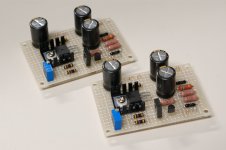
Build details:
Q1 = J202
Q2 = BD140
Q3 = 2SK213
R1, R8 = 75k Welwyn
R2 = 475R||475R = 237.5R Vishay 1/2W
R3 = 4k75 Vishay 1/2W
R4, R6, R9 = 47R Kamaya carbon
R5 = Vishay 1k trim
R7 = 150 ohm 2 W, Vishay PR02
C1,2,3 = Nichicon KZ 100u 50V (yeah, those. I splurged...)
Attachments
Last edited:
Gimme a couple of weeks. The boards will be here then.
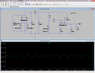
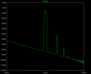
I'd like to digress one second and discuss the distortion produced by this circuit. This is not a "clean" amplifier. Single-ended FET followers with resistors rather than current sources have a sound, characteristic of the circuit, pleasant, but not strictly transparent.
Simply put, the resistor isn't as good as the FET at supplying current so the waveform output ends up asymmetric, it compresses slightly around the crests of the negative current half. Interestingly, it does so regardless of whether the waveform amplitude is large or small.
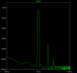
As an Fourrier transform, what you see is a distortion spectrum with the second harmonic at 0.5% of fundamental, and the third harmonic at 0.05% of fundamental (for 32 ohm headphones). This pattern is, once you back off hard clipping, invariant of amplitude. i.e. distortion level is mostly independent of output power.
The Sziklai input stage is pretty much a FET follower, and shares the same distortion characteristics, but always much lower in level than those of the output stage, so they make no contribution to the total. The Sziklai appears to add no new higher order components, either.
This is what the simulation says, and the circuit is basic enough that I'm confident the software is essentially producing the correct result. The whole thing is dominated by the output MOSFET stage.
So, that's fine, actually. I think this very simple, constant distortion pattern should sound really good and enjoyable, despite the relatively high numerical value of the THD. That's what I'm aiming to verify, confirm if you will.
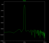
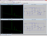
Typical output distortion pattern (32 ohms) shown below. That's what you see no matter what, so if you don't like it don't build this amp! For comparison, also shown is 32 ohms load on a LT1028 op amp non-inverting, same gain setting. Well, well. Gotta have faith, right?
I'd like to digress one second and discuss the distortion produced by this circuit. This is not a "clean" amplifier. Single-ended FET followers with resistors rather than current sources have a sound, characteristic of the circuit, pleasant, but not strictly transparent.
Simply put, the resistor isn't as good as the FET at supplying current so the waveform output ends up asymmetric, it compresses slightly around the crests of the negative current half. Interestingly, it does so regardless of whether the waveform amplitude is large or small.
As an Fourrier transform, what you see is a distortion spectrum with the second harmonic at 0.5% of fundamental, and the third harmonic at 0.05% of fundamental (for 32 ohm headphones). This pattern is, once you back off hard clipping, invariant of amplitude. i.e. distortion level is mostly independent of output power.
The Sziklai input stage is pretty much a FET follower, and shares the same distortion characteristics, but always much lower in level than those of the output stage, so they make no contribution to the total. The Sziklai appears to add no new higher order components, either.
This is what the simulation says, and the circuit is basic enough that I'm confident the software is essentially producing the correct result. The whole thing is dominated by the output MOSFET stage.
So, that's fine, actually. I think this very simple, constant distortion pattern should sound really good and enjoyable, despite the relatively high numerical value of the THD. That's what I'm aiming to verify, confirm if you will.
Typical output distortion pattern (32 ohms) shown below. That's what you see no matter what, so if you don't like it don't build this amp! For comparison, also shown is 32 ohms load on a LT1028 op amp non-inverting, same gain setting. Well, well. Gotta have faith, right?
Attachments
Last edited:
Yes, that's like simonov was suggesting, and it will will certainly work to reduce the total distortion figure.
Then, so will will using an op amp.
I whipped up your schematic in LTSPice, and the distortion spectrum with a CSS is shown below.
It would be interesting to try, definitely. You could use the boards I made, replace the resistor R7 with the CCS on a tiny daughterboard.
Then, so will will using an op amp.
I whipped up your schematic in LTSPice, and the distortion spectrum with a CSS is shown below.
It would be interesting to try, definitely. You could use the boards I made, replace the resistor R7 with the CCS on a tiny daughterboard.
Attachments
Last edited:
I left the headphone load at 300 ohms by mistake in that last sim, rather than changing to 32 ohms. Also forgot to check the bias current.
On apples-to-apples, adjusting the CCS until the bias current is the same as with the simple source resistor, I see the following improvement on going to the CSS. Not quite as radical, but definitely there.
On apples-to-apples, adjusting the CCS until the bias current is the same as with the simple source resistor, I see the following improvement on going to the CSS. Not quite as radical, but definitely there.
Attachments
Last edited:
As you probably know, a CSS acts like a small resistor when supplying current, and like a big resistor when providing a load. To first order that's all we are seeing here.
The MOSFET sees a combined load of the CCS/source resistor in parallel with the headphone impedance. It's dominated by the smaller of the two values. There is only limited benefit, therefore, in making the CSS effective load resistance much higher than the headphone impedance.
Instead the CSS is more about efficiency: you can provide the source impedance comparable to the 33ohm resistor but run at a much lower voltage, saving power.
That's important for something like the Pass Zen circuit where we are talking perhaps 50 watts power savings, but here the difference is more like 500 mW. My take on the CSS is that with respect to the J-Mo mk ii circuit, it is desirable from an efficiency standpoint but it is not expected to drastically improve the sound.
Last edited:
- Status
- This old topic is closed. If you want to reopen this topic, contact a moderator using the "Report Post" button.
- Home
- Amplifiers
- Headphone Systems
- J-Mo Mk II headphone amplifier