R4 is a safety, preventing the total resistance from falling below 47 ohms even if the trimmer is (accidentally) turned to zero. I'd rather you kept it in.
R9 with C3,C4 is a filter, to reduce noise and ripple from the input stage. It is not "mission critical".
re. the 2SK170, I checked out the datasheet and realized I was mistaken: it's a low current JFET, more like the 2N5484 than the 2N5486. Short story is its good when you want to increase the circuit gain (like I did for my 300 ohm headphones) but it wont work at the 3:1 R3:R2 ratio shown in the official schematic/BOM.
Roughly speaking, it works out as follows:
175 mA source current is desired, and the resistance is 30 ohms. The MOSFET source should therefore be at 5.25 V. The MOSFET gate ends up (for the IRF510 and similar) about 4 V higher, so 9 V. The working source voltage of the JFET is the MOSFET gate voltage multiplied by the voltage divider R2/(R2+R3) [1/4], so 9/4 or 2.25 V.
To work properly, the JFET must therefore have a Vp safely in excess of 2.25 V.
Not coincidentally, the circuit gain is also defined by the voltage divider R2/(R2+R3), as the inverse (R2+R3)/R2 aka 1+R3/R2, though in practice there are additional losses in the circuit that reduce the total somewhat.
Last edited:
Thank you again.... that explanation is what I needed ")
All values are in the ballpark.
Finished soldering and connected the rig to the preamp output.... It works... no audible distortion, no hum, suitable sound preassure... Now must build the other channel so I can do a comparative listening test.
All values are in the ballpark.
Finished soldering and connected the rig to the preamp output.... It works... no audible distortion, no hum, suitable sound preassure... Now must build the other channel so I can do a comparative listening test.
I have been listening with 30ohm AKG phones and it sounds really good.
I had to power each channel with it's own BiB because of total power consumption.
Super silent, agile bass, extended and very clean trebble, quite outstanding attack.
I am not very experienced with headphone preamps but it seems very difficult to beat.
Now I would like to make it suitable also for higher impedance phones.... can it be done easily ?
Glad you like it!
It can be modified for higher impedance headphones, but not as easy as just changing a resistor.
There are two things:
1. adjust the output stage for more voltage and less current.
2. increase the voltage gain.
You have to re-build the circuit using a FET with lower Vp. Change the ratio R3/R2 to something like 10:1. Increase the power supply to 25 V. Increase the source resistance to 150 ohms. Adjust the operating point so that the MOSFET source is 12 V.
Glad you like it!
It can be modified for higher impedance headphones, but not as easy as just changing a resistor.
There are two things:
1. adjust the output stage for more voltage and less current.
2. increase the voltage gain.
You have to re-build the circuit using a FET with lower Vp. Change the ratio R3/R2 to something like 10:1. Increase the power supply to 25 V. Increase the source resistance to 150 ohms. Adjust the operating point so that the MOSFET source is 12 V.
Is this ok to drive 300ohm headphones ?
I have been reading about the complementary Darlington and now it seems clear to me that gain is set mainly by the feedback resistor R3.
According to your indications
"circuit gain is also defined by the voltage divider R2/(R2+R3), as the inverse (R2+R3)/R2 aka 1+R3/R2"
"175 mA source current is desired, and the resistance is 30 ohms. The MOSFET source should therefore be at 5.25 V. The MOSFET gate ends up (for the IRF510 and similar) about 4 V higher, so 9 V. The working source voltage of the JFET is the MOSFET gate voltage multiplied by the voltage divider R2/(R2+R3) [1/4], so 9/4 or 2.25 V."
This works in your low impedance schematic but in my case I have:
R3 = 1k5
R2 = 220
Q3 gate = 9.97v
Q3 Source = 5.37v
Q1 source = 2.53v
R2 / (R1 + R2) = 0.128
0.128 x Q3 gate (9.97) = 1.28
So using your formulae I can not get the real Q1 source = 2.53
Last edited:
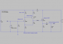
Ok, here's the circuit as I built it for myself, for HD-600 (300 ohms).
I used J202, BD136, and 2SK213. The gain is defined as 4750/235+1, but the gain programmed by the voltage divider is getting a bit too close to the "open loop" maximum so the actual gain is a bit lower than expected, about 15x. The current through the JFET and PNP are both in the 2-3 mA range.
I'm not sure what the currents in the input stage should be ideally. Of course the available range depends on the model of JFET. I've tried to adjust the resistors so that the currents in both devices are about equal.
FYI the Vs of the J202 ended up about 0.7~0.8 V.
Attachments
Last edited:
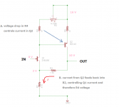
Would you please explain how first stage works so I can better visualize the mods ?
This may or may not be of some assistance:
Attachments
The circuit block distorts least at unity and low gains. The distortion, however, is anyway below the MOSFET output stage, so we don't care. It's also, like the MOSFET follower, dominant 2nd harmonic.
If we did care, we'd have to do something different for voltage gain. An op amp, for instance.
Fun thought: Take the Sziklai stage above, make it unity gain, and replace the jfet with a npn transistor. Then mirror the whole thing across the ground line, so it's push-pull buffer. That's a headphone driver in and of itself, right there.
- Status
- This old topic is closed. If you want to reopen this topic, contact a moderator using the "Report Post" button.
- Home
- Amplifiers
- Headphone Systems
- J-Mo Mk II headphone amplifier