Hello, Richard !!!
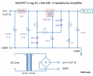
I just built the amplifier and have a question to you. I worked with the schematic in your post 311. My JFET's are matched, I measured Vgs0=3,56V for the first one and Vgs0=3,6V for the second one. According to your xls-table, I calculated R2=430R. Today assembled the PCB's and try to adjust the bias current of the MOSFET. But here I found a problem. The trim pot turns ended, but the source voltage can't reach desired 5,5V. With full resistance of the trim pots, the bias current is about 150mA for both MOSFET's (about 5V source voltage). The supply voltage is 16,2V from regulated PSU. Can you give me an advise what to do, please.
Thank you !
Last edited:
Hi,
Depending on what measurement method you used, a measured V_gs0 of 3.6V may not correspond to what I was using for the estimates built into the worksheet. It seems that your FETs have the wrong properties for the resistors used, so you'll have to change either the resistor values or the FETs.
If you are not too concerned about a small change in voltage gain, I think the easiest adjustment is R2. Ideally you'll want a value that gives 5.5V on the MOSFET source when the trim pot is approximately centered.
As far as I can tell, your V_gs0 values are lower than I anticipated and R2 must be deceased to bring the output offset into the adjustment range. I believe the BOM value of R2 = 332 ohms or thereabouts should be close to the value you will need, but you may need to adjust via. trial and error.
The circuit gain will increase a little bit from what it is now.
(It's been a while, I had to think a bit about what a lower-than-anticipated source voltage means about the FET pinch off voltage and what direction the adjustment work in. I find the circuit is counter-intuitive, and tend to use LTSpice to examine the behavior rather than try to work it out by hand.)
Hi, Richard !
I used your method with 9V battery and 2 different resistors to measure Vgso and Idss, made calculations with your xls-table. I will try to reduce R2 value to 330R and will report the behavior of the schematic. Bought 10pcs of JFET's and my best pair is with measured Vgso=4,17V. I used the pair with the lowest Vgso, the other 4 pairs are with higher Vgso.
Thank you very much for the advice !
Best Regards !
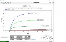
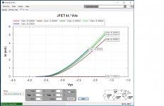
I'm not sure which worksheet you are referring to - it's been quite some time since I last looked at this circuit. The one I found, attached for your reference, suggests a R2 value of 330 ohms when the FET -V_gs0 is about 3.6 V, while a larger value 420 ohms would needed for -V_gs0 of 4 V or so.
The worksheet calculations are idealized but should work nicely when the Vgs0 values are computed using my "two step" method rather than a commercial tester. A safer bet is to measure the gate source voltage with the "R_match" value shown in the worksheet and compare that -V_gs voltage with the table values directly rather than the -V_gs0.
The worksheet calculations are idealized but should work nicely when the Vgs0 values are computed using my "two step" method rather than a commercial tester. A safer bet is to measure the gate source voltage with the "R_match" value shown in the worksheet and compare that -V_gs voltage with the table values directly rather than the -V_gs0.
Attachments
The amplifier is not better tnah its power supply. Driven by this principle, last two days made experiments with different types of PSU. First type-LM317 regulated PSU. Sounds aggressively. Second type-the same+additional RC circuit 1R and 10000uF. Sounds much better, but again far from my understandings for natural sound. Today started to try unregulated PSU's. For begining I made CRCRCRC filter after the rectifier. I used transformer with 20Vac otput voltage and 22000uF capacitors+10R/2W resistors. Sound-oooooooh yesssss, we started to move in right direction. All aggression is in the past. Sound is smooth, warm and pleasant.
Conclusion from the test till now-the amplifier is very transparent sounding and very sensitive to its PSU. I think the regulation "needles" from the operation of the voltage regulator are the main reason for nonpleasant result in sound. I want to try full wave rectifier (two secondary winding of the transformer+two diodes). And some more extras...
Conclusion from the test till now-the amplifier is very transparent sounding and very sensitive to its PSU. I think the regulation "needles" from the operation of the voltage regulator are the main reason for nonpleasant result in sound. I want to try full wave rectifier (two secondary winding of the transformer+two diodes). And some more extras...
In this particular case-no, I didn't. But I am very familiar with this type PSU, because I have a lot of experience with it. I used the same schematic, but with IRF730/IRF740/IRF830/IRF840, for high voltage power supply in vacuum tube amplifier's stages. I experimented with other similar schematics like the "virtual battery" by Andrea Ciufolli, capacitance multiplier by Rod Elliot and many others with MOSFET's, Darlington's, with Zener diodes in gate/base circuit, withouth Zener diodes, etc. All sounds similar and have got problems with the width/depth of the sound scene. After a lot of experiments and lost time/money, I learned that less active elements in the circuit means better sound.
What do you think about possible subtitution of the JFET's. It's very easy and cheap for me to find J211 and J111. I watched the datasheets and J211 seems to be close to 2N5486, with Vgso(min)=-2,5V and Vgso(max)=-4,5V. The pins arrangement is the same for direct change and listening tests. Even I think to mount pins, extracted from DIP-8 opamp socket and to change tne JFET's withouth soldering.
I searched for better output MOSFET with lower input capacitance, too. Seems that IRF610 have 135pF input capacitance versus 180pF for IRF510, but Rds(on) is lower for IRF510.
I searched for better output MOSFET with lower input capacitance, too. Seems that IRF610 have 135pF input capacitance versus 180pF for IRF510, but Rds(on) is lower for IRF510.
Substitution of the JFET allows you to adjust ratio of the voltage gain to DC bias. Since you normally want to keep the DC output bias fixed at 5.5 V, it gives you the flexibility to build a version of the JMo2 with lower or higher voltage gain range, using JFETs with higher or lower -V_gs0 value respectively, keeping the circuit currents otherwise constant.
So if you have available JFETs in the range that you want, by all means use them.
That said the circuit works best at low gains (more degenerative feedback, lower distortion) which means you want a JFET that runs at about 1.5~2 mA when -2 to -6 V gate voltage is applied.
As for the MOSFET, the compound FET-Bipolar input stage has a low output impedance and can easily drive most power MOSFETs through the audio bandwidth. A MOSFET with low input capacitance is desirable to a point but there is no need to minimize this parameter.
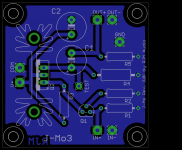
J-Mo 3
Some new thoughts on this, enough to start a new version "J-Mo 3".
I dropped the bipolar transistor from the circuit. While it helped the PSRR a little, it didn't really pull its weight. The J-Mo 3 is back to a two stage JFET-MOSFET design, but unlike the original the FET is configured as an amplifier and not a follower so the circuit has voltage gain.
The amount of voltage gain can be adjusted by playing around with the power supply voltage and the value of R3.
This is a really small board, 5x5cm. Single-sided, at least functionally, I might double the ground later at fabrication.
Acknowledgement here to the pocket class A project by xrk971 for some helpful ideas.
Attachments
Last edited:
Hello Richard
I want to build a 20dB gain stage to use as MC pre pre before my MM phono preamp.
I already built your headphone amp and based my self on your design to have something similar but with more gain.
I know you have more experience than most with these topologies so I would really apreciate your input here: http://www.diyaudio.com/forums/solid-state/323937-sziklai-jfet-input-mc-pre-pre.html#post5463337
Best
Ricardo
- Status
- This old topic is closed. If you want to reopen this topic, contact a moderator using the "Report Post" button.
- Home
- Amplifiers
- Headphone Systems
- J-Mo Mk II headphone amplifier