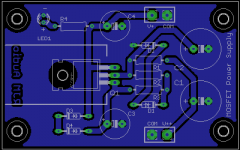
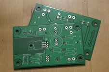
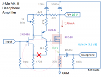
Mosfet voltage regulator circuit
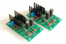
This is the "suggested" voltage regulator to use with the J-Mo mk ii. It's a sister board to the main circuit, same size and mounting, same basic layout for the IRF510.
The Zeners are all 10 V. The output is 16 V DC, with a 1s soft start. The LED isn't needed, but since there should be some loading to allow the output to bleed quickly to 0 V on shut down, I figured might as well have an indicator light.
The IRF510 gate is protected from overvoltage by Zeners, and R1 gives some measure of overcurrent protection, worse case it acts as a sacrificial fuse.
The output ripple depends on the current draw of course, but it's quite low: about 0.25 mV at 200 mA output.
As configured, it drives one J-Mo channel. For stereo, R1 should be reduced to 5 ohms.
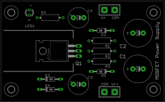
Attachments
Last edited:
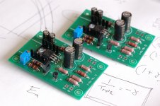
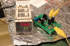
Thermals
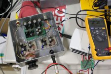
Powered up and running as simulated. Excellent control of the bias current via the trimmer resistor.
With 16-20 V V++ and 180 mA bias current the MOSFET will dissipate 1.9-2.7 W.
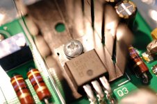
I tried using Aavid 507302B00000G heatsink with the IRF510. It's rated at 24 C/W. For an ambient of 30 C, the MOSFET is expected to reach 75-95 C. I measured it at a couple of operating points and verified that this was indeed the case. (see photo)
The IRF510 is fine up to 150 C, so it's operating well within spec, but nevertheless the heatsink is a bit marginal... once the boards are in an small enclosure, and if people start running at over the rated bias current, things will rapidly get unpleasant.
The Aavid 504222B00000G (shown below) should substitute just fine on the PCB, and has a thermal resistance of only 6 C/W. MOSFET temperatures should, with this heatsink, stay under 50 C. I'll order a few and try them out.
Powered up and running as simulated. Excellent control of the bias current via the trimmer resistor.
With 16-20 V V++ and 180 mA bias current the MOSFET will dissipate 1.9-2.7 W.
I tried using Aavid 507302B00000G heatsink with the IRF510. It's rated at 24 C/W. For an ambient of 30 C, the MOSFET is expected to reach 75-95 C. I measured it at a couple of operating points and verified that this was indeed the case. (see photo)
The IRF510 is fine up to 150 C, so it's operating well within spec, but nevertheless the heatsink is a bit marginal... once the boards are in an small enclosure, and if people start running at over the rated bias current, things will rapidly get unpleasant.
The Aavid 504222B00000G (shown below) should substitute just fine on the PCB, and has a thermal resistance of only 6 C/W. MOSFET temperatures should, with this heatsink, stay under 50 C. I'll order a few and try them out.
Attachments
Last edited:
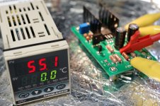
The addition of the new heatsink reduced the temperatures down to the 50-75 C range, MOSFET case temp is 55 C at the standard operating point V+ = 16 V, Vs = 5.5 V, Rs = 30 ohms.
The temperature of the MOSFET case are a somewhat higher than anticipated based on the heatsink thermal conductivity. The specification is 6 C/W (which struck me as optimistic), while the actual temperatures suggest 15 C/W. No big deal, but just a memo that specifications vs. reality for heatsinks seems to be a bit hit-or-miss.
The temperature of the MOSFET case are a somewhat higher than anticipated based on the heatsink thermal conductivity. The specification is 6 C/W (which struck me as optimistic), while the actual temperatures suggest 15 C/W. No big deal, but just a memo that specifications vs. reality for heatsinks seems to be a bit hit-or-miss.
Attachments
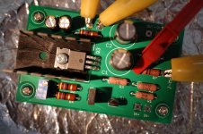
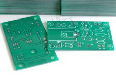
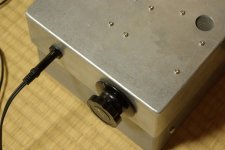
For the boards, there are several options: Screw terminals, a length of wire lead, gold pin, as well directly soldering the wire to the pad. For perf-board, I usually make a loop of wire around two adjacent pads and either solder a lead wire to the loop or, for example, attach test leads by alligator clips.
Hi, I wonder if you could post the values you use for components, different to those stated on your website for use of this amp with your 300ohm 'phones? (including the power supply if any different)
I have had a look through the thread but the component names seem to be different to the final design on the site (might just be me).
Also what values would you use for 600 ohm phones?
Thanks!
I have had a look through the thread but the component names seem to be different to the final design on the site (might just be me).
Also what values would you use for 600 ohm phones?
Thanks!
Sorry for taking such a long time to get back on this.
I built a prototype on perf board, to match 300 ohm headphones and my available power supply (24 VAC), in post 34. The LTSPICE file is attached.
The parts numbering are consistent with the web page, but the values are changed to fit not just my headphones, but also the different jFET and MOSFET transistors I used. The 2SK213, in particular, has very different Vgs from the IRF510.
It's a drawback of this circuit that it does not suffer modifications gladly. Change one component, and all the others have to be adjusted slightly to match. This is most easily done in LTSPICE.
The general aim when adjusting for higher impedance headphones is to increase the voltage rail, increase the gain, and decrease the bias current. The source resistor R7 should be increased to approximately the value of the headphone impedance, and the voltage rail increased until about 0.5 W is dissipated in both R7 and the MOSFET.
I should emphasize that this is an optimization, it is not necessary to change the values from the circuit shown in the web page even when using 300 ohm headphones, it just increases the available output power into the specified load.
I built a prototype on perf board, to match 300 ohm headphones and my available power supply (24 VAC), in post 34. The LTSPICE file is attached.
Q1 = J202
Q2 = BD140
Q3 = 2SK213
R1, R8 = 75k Welwyn
R2 = 475R||475R = 237.5R Vishay 1/2W
R3 = 4k75 Vishay 1/2W
R4, R6, R9 = 47R Kamaya carbon
R5 = Vishay 1k trim
R7 = 150 ohm 2 W, Vishay PR02
C1,2,3 = Nichicon KZ 100u 50V
The parts numbering are consistent with the web page, but the values are changed to fit not just my headphones, but also the different jFET and MOSFET transistors I used. The 2SK213, in particular, has very different Vgs from the IRF510.
It's a drawback of this circuit that it does not suffer modifications gladly. Change one component, and all the others have to be adjusted slightly to match. This is most easily done in LTSPICE.
The general aim when adjusting for higher impedance headphones is to increase the voltage rail, increase the gain, and decrease the bias current. The source resistor R7 should be increased to approximately the value of the headphone impedance, and the voltage rail increased until about 0.5 W is dissipated in both R7 and the MOSFET.
I should emphasize that this is an optimization, it is not necessary to change the values from the circuit shown in the web page even when using 300 ohm headphones, it just increases the available output power into the specified load.
Attachments
This is proving to be more pernicious than usual.
Changed out jFET, pnp, and MOSFET on the channel with abnormally high gain (and unstable bias). No effect. Still getting +8 dB (2.5x), and a gain that varies wildly with the trim resistor position. Does not behave like the "good" channel, yet the DC voltages / currents are all nominally correct (but consistently Vgs is about 100 mV less). Triple checked the board layout for mistakes and cold solder joints, no joy there.
I'm coming to the inevitable conclusion that the circuit operating points are borderline, and that the amplifier section can slide out of the "control region" where the behavior is described by simulation to some other state...
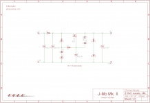
Fault traced to a bad solder joint, position shown in the schematic below.
Fixed! (big sigh of relief...)
I'll let them burn in (I replaced most of the silicon before I finally clued in to the problem) and trim the bias currents before reporting the final channel balance, but it looks to be very, very close.
Should be able to do trial listening tonight...
Fixed! (big sigh of relief...)
I'll let them burn in (I replaced most of the silicon before I finally clued in to the problem) and trim the bias currents before reporting the final channel balance, but it looks to be very, very close.
Should be able to do trial listening tonight...
Attachments
J-Mo Mk. II development: Feb 2012 - Apr 2013.
Finally, up and running properly.
With the bias currents matched, the AC gains are matched to within 0.5%, or 0.04 dB. If really want, you can trim the bias to match the AC gains even further. Channel balance is in any event a non-issue.
Finally, up and running properly.
With the bias currents matched, the AC gains are matched to within 0.5%, or 0.04 dB. If really want, you can trim the bias to match the AC gains even further. Channel balance is in any event a non-issue.
Attachments
Last edited:
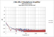
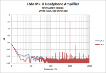
Measurements.
330 ohm load, since my optimization of the circuit is for my 300 ohm headphones. The circuit gain is 23 dB (14x).
With no input, the noise baseline is a ridiculously clean -130 dB.
With 100 mV (1 kHz) into 330 ohms, the 2nd harmonic is at -90 dB, or -70 dB below the fundamental. 0.03% distortion. The large second harmonic component was expected for this single-ended output topology. And it's not even that large. 3rd harmonic and all higher harmonics are below -110 dB, the peaks shown in the plot are most likely artifacts of the signal generator.
The results are actually pretty nice...
Attachments
- Status
- This old topic is closed. If you want to reopen this topic, contact a moderator using the "Report Post" button.
- Home
- Amplifiers
- Headphone Systems
- J-Mo Mk II headphone amplifier