Hello all!
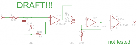
I'll need your advice on building a headphone amp and pream in one with initial schematic attached (just an idea, do not implement it as something working).
Ok, here's the whole idea:
- Input from CD player, DAC or (less likely) PC Soundcard.
- Gain stage with AD8599BRZ. Chosen as I have one or two of them around and they are best used with low input impedance (<1k ohm).
- Potentiometer (will be using Panasonic EVJ). It's placed after the OpAmp as to provide constant, low impedance of the source to AD8599.
- I/V stage with LME49720 at unity gain (could't find that in LME's DS, hope it is UG stable). Though I'm not sure about if it is needed at all.
- Discrete bipolar buffer (IC Buffer on schematic used only for illustration)- haven't chosen any particular implementation yet. Purpose: driving cables and headphones, providing high impedance for OpAmps, delivering current. Requisite: low output impedance.
I would like to kindly ask you for your recommendations and feedback.
Thanks,
GLooP
Attachments
I think R4 needs to be moved into the feedback loop and the connection to ground where it was needs to be eliminated for unity gain... I think.
I'm not a fan of discrete output for headphones. The impedance is rarely low enough for what modern data suggests is good enough, <1Ω.
Also, I'm wondering why you need an I/V stage? Are you not taking line input but taking feed straight from DAC? In that case, yeah... get an I/V stage going. I'd use the LME49740 and include the other two opamps from that package in the feedback loop for the AD8599 and buffer, or use the AD8599 in the feedback loop of the LME49740.
Are you planning to design a circuit that feeds speaker amp and headphones at the same time or just have a selector switch?
I'm afraid that circuit won't work....as shown. The input op-amp doesn't have a correct feedback configuration and will just swing rail-to-rail with minimal input.
Yes, you should include the BUF04 in the feedback loop for IC2. R4, and another resistor, could provide some gain if you need it.
Cheers,
Dave.
Yes, you should include the BUF04 in the feedback loop for IC2. R4, and another resistor, could provide some gain if you need it.
Cheers,
Dave.
Thank you Davey and ethanolson!
Strangely, the feedback is really missing for AD8599. There should be a 1,4k feedback resistor from inverting pin to the output, constituting total gain of ~ 4 for the first stage, somehow I've probably deleted it.
Having AD8599 its own local feedback and before the volume pot is done so by purpose as this part has really nice input figures: 1.15nV/rtHz. This is quite close to AD797's 0.9 nV/rtHz and I wish to make some use of it (it's clear I cannot achieve it, but still). Also, once again - AD8599 is designed to work with lower than 1K ohm input impedance so it have to be fet directly from source. This makes the global feeback problematic.
I've put a second OpAmp as I was not sure if it is a good idea to provide constant input impedance to the buffer. If I omit the second OpAmp, potentiometer's position will determine the input resistance buffer sees and I'm not sure how this will result.
I've made several mistakes on the schematic and I'll correct them when I have more time, but the idea is:
* AD8599 has to have 1,4k feedback resistor
* LME49720's feedback is at the buffer's output
* R4 is referenced to non-inverting, instead of inverting pin
* Buffer is going to be some discrete solution like Jung's buffer or just a single follower with current sink. Haven't decided yet.
I would appreciate your thoughts on:
1) Topology [OpAmp]-Pot-[OpAmp-Buffer] (where [] shows feedback loop)
2) Is IC2A = LME49720 actually needed?
3) What buffer should be best - some kind of diamond buffer (i.e. Jung's) or simple follower+sink? Required ouput current as high as 120 mA.
Thank you,
GLooP
I think if you used a diamond type buffer then you can omit the second opamp. With the gain stage before the volume pot, there is a potential for clipping the first opamp, thus producing a lot of distortion besides the fact that you'll be throwing away a lot of gain. A better arrangement might be: Buffer -> volume pot -> gain stage -> buffer -> output.
Last edited:
I'm losing performance if I put a volume pot before the gainstage. Clipping is not expected to be an issue; AD8599 should be able to produce +/- 10V peak voltage swing at +/- 12V supply. Meaning clipping is going to be a problem at higher than +/-2.5V. This is safely above line level of 1V rms so I do not expect problems here. Again - the purpose of this amp will be to be placed between a DAC or CD player and input volume is expected to be low and the amp will douple preamplifier and headphone amplifier.
If I have the time, I might try it with NE5532 or TL072 instead")
If I have the time, I might try it with NE5532 or TL072 instead
I think most CD players will put out 2volts max. At the least, you'll have higher distortion with higher output from the opamp. Historically, most designs put the gain stage after the volume pot and fancy designs put a buffer ahead of the volume pot also, as well as a buffer after the gain stage. But, it's a free world, go ahead and experiment.
I think most CD players will put out 2volts max. At the least, you'll have higher distortion with higher output from the opamp. Historically, most designs put the gain stage after the volume pot and fancy designs put a buffer ahead of the volume pot also, as well as a buffer after the gain stage. But, it's a free world, go ahead and experiment.
Actually, I have only my USB DAC right now and the Dac IC is not buffered. So this topology will blend greatly since most DACs are buffered then there is the volume pot and the amp. What I do is adding a gain stage which will buffer the DAC and then implement a amplifier, whill will be then responsible to drive cables' capacitance safetly. I have not reinvented the wheel, even O2 is constituted this way - gain-pot-I/V.
BTW: I really appreciate your input, dirkwright, thank you!!!
Last edited:
Better don't omit R4 as suggested, it limits pot scratching. Do include a coupling cap in between the pot and R4, else you'll have input bias current flowing through it, which may turn it into a scratch fest.
If in doubt, I'd rather swap the values of R6 and R12 (or make both 100R), power transistors can have a good bit of input capacitance. Any reason you're using a SE output stage with CS instead of a push-pull affair?
I'd distribute gain in between the two stages. Having gain only in the first one gives phenominally low noise but is a little fussy to work with in the real world. Remember that the input may have to accept up to 2.5 Vrms + 3 dB to account for intersample-overs (about 3.25 Vrms), so I wouldn't give it a lot more gain than 6 dB when running on +/- 12V.
As far as using a super low Vnoise OP in the input is concerned, it's probably a waste. Ever bothered calculating source noise? Besides, this is a line-level stage that has to handle levels in the Vrms range, so it will offer plenty of instantaneous dynamic range in any case. This is not the case for the second stage, where even the output may only be in the mV range.
- Status
- This old topic is closed. If you want to reopen this topic, contact a moderator using the "Report Post" button.
- Home
- Amplifiers
- Headphone Systems
- Preamp and Headamp 2 in 1?