The O2 charging circuit is a current limited constant voltage design of the most basic kind. It is only suitable for Ni Cad and Nickel Metal Hydride types, not Lithium Ion. It has around 11.2 volts available open circuit. The higher the cell voltage reaches, the lower the current becomes... it is a tapered charge.
Lithium Ion cells must be charged with a circuit that cuts off the current when full charge is reached. You also can not trickle charge them... it destroys them in very quickly.
Lithium Ion cells must be charged with a circuit that cuts off the current when full charge is reached. You also can not trickle charge them... it destroys them in very quickly.
remote power switch
hi everyone,
i would like to mount the switch remotely but i cant figure out which pins go where.
would this switch do the trick?
what do i have to connect where?
Thanks.
hi everyone,
i would like to mount the switch remotely but i cant figure out which pins go where.
would this switch do the trick?
what do i have to connect where?
Thanks.
But without charging (taking the batteries off for charging) how long run time from using the 18650's? Or does it need some regulator much current?
I looked up the batteries and they are rated at 3000mAh. So if you measure the current draw per rail and divide that into 3000 you get you run time in hours.
I would guess for the 3 opamps and a comparator you are probably looking at 150 to 200 hours depending how loud you play it.
hi everyone,
i would like to mount the switch remotely but i cant figure out which pins go where.
would this switch do the trick?
what do i have to connect where?
Thanks.
It seems OK although the description is poor. It needs to be a double pole double throw type (6 pins in total).
Wiring it is easy.
The middle pin on one side of the switch goes to the power supply (junction D1 and D2). The top pin on the same side goes to pin 8 of the comparator (look at the circuit).
The other middle pin goes to D5 and D6. The top pin of that side goes to pin 4 of the comparator.
Hello, been lurking a long time here but finally time to post.
I tried OPA1662's as output chips on my O2, after reading about it here: http://www.diyaudio.com/forums/head...ersion-o2-desktop-amp-oda-69.html#post4191566
However, my DC offset rose to 53.5 and 55 mV. With stock JRC4556 I have only 3.5 mV offset and with LME49720, 1.5 mV both channels.
Now OPA1662 have a lot higher offset and bias currents than 4556, but I'm still surprised. Can anyone confirm this is enough for the big difference or is something else going on?
Attachments
It sounds high but not beyond the bounds of possibility given the specs of the device. Worst case of 1200nA across the 40.2k would give 48mv and on top of that there is a possible imbalance in input offset currents to make things worse.
Try shorting R12 (or R13) and see what the offset falls down to.
Try shorting R12 (or R13) and see what the offset falls down to.
It sounds high but not beyond the bounds of possibility given the specs of the device. Worst case of 1200nA across the 40.2k would give 48mv and on top of that there is a possible imbalance in input offset currents to make things worse.
Try shorting R12 (or R13) and see what the offset falls down to.
Hi Mooly. I shorted R12 and DC offset is down to -0.5 mV. Other channel stayed at 53.5 mV.
Interesting. So it looks like this is going to be normal behaviour and purely the result of the relatively high input bias currents for these devices causing this offset. The good news is that although it sounds high, in reality little current will flow into a typical headphone DC resistance. You can measure how much for your particular headphone by measuring the volt drop across one of the 1 ohm resistors of the appropriate channel and calculating using ohms law. The voltage will be very tiny though and perhaps not resolvable on a typical DVM.
If the phones have say 20 ohm DC resistance then something around 2.5ma would flow.
No easy fix I'm afraid although it could be made 'better' by lowering impedances of the surrounding circuitry.
If the phones have say 20 ohm DC resistance then something around 2.5ma would flow.
No easy fix I'm afraid although it could be made 'better' by lowering impedances of the surrounding circuitry.
Although I say there isn't an easy fix... well the 'obvious' one would be to add a similar value resistor to R12 and R13 into the feedback path to equalise the error and make both inputs see the same offset voltage. You would have to do it for all four opamps. The downside of this is that the opamp node becomes sensitive to stray noise pickup, and also the step response (squarewave testing) of the circuit could be altered although probably not in any audible way.
Attachments
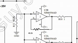
Thx for the info! I actually went ahead with a compromise and replaced R12 and R13 with 30k resistors. (38 mV offset now). I won't do any advanced modifications, so probably the original opamps but with gain stage LME49720, will be going back in soon. Listening to the amp now with my HD650's and indeed the sound is different.
Instead of going electrolytic, can you solder MKP caps in parallel?Sounds like a plan
You could also decrease the resistor by a factor of 5, increase the 2.2uF coupling cap to 10uF (so an electrolytic) and decrease the volume control to a 2k (or 2k2). That would preserve the low frequency response and reduce the offset significantly.
Although I say there isn't an easy fix... well the 'obvious' one would be to add a similar value resistor to R12 and R13 into the feedback path to equalise the error and make both inputs see the same offset voltage. You would have to do it for all four opamps. The downside of this is that the opamp node becomes sensitive to stray noise pickup, and also the step response (squarewave testing) of the circuit could be altered although probably not in any audible way.
Hi again, I didn't really feel good with leaving 30+ mV offset...
I did this modification after realising I can keep it all on the adapter boards - no need for cutting traces on the actual amp. So I cut leg 2 and 6 just before it enters the socket and soldered 80k SMD resistors between pin 1&2 and 6&7.
It works! 1 mV DC offset! However I got oscillation due to the decreased phase margin (yeah I've read a bit about this). IC temp was all they way up to 64°C, although music sounded fine.
Soldering a no-name salvaged 56 pF ceramic as a phase compensating cap parallel to the resistors seems to fix the issue. IC temp is down to 39 °C after playing loud music 1 hour into my cheaper 60 ohm cans.
My question is, does the quality of the capacitor matter? There's so many choices, although in the 10-50 pF range (to stay above 30 kHz -3db) I can easiest find MLCC NP0 caps for cheap.
Attachments
The quality of the cap should make no real difference.
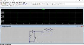
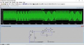
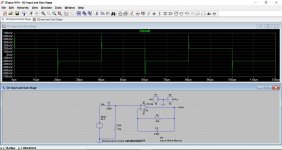
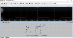
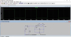
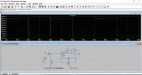
There is another way of looking at this though. The cap value isn't critical because it is working into an amp configured for unity gain. We can simulate this quite well using a high speed opamp and using a squarewave test source.
Image 1 is the baseline performance.
Image 2 is with the resistor in place. The circuit oscillates.
Image 3 is with just 2.2pF added.
Image 4 is with 22pF. The circuit is stable but not still at the 'baseline' level.
Image 5 is with a much larger 1uF cap added. We have now matched the baseline performance and as a bonus, the cap ensures the input pin is tied to the low output impedance of the opamp output at AC. This means the pin is not susceptable to stray noise pickup.
In other words if you to touch the pin with the resistor and a tiny cap in place then the opamp will hum and buzz loudly. Do the same with a large cap fitted and it will not.
Image 6 is with 2200pF cap (as requested") )
)
There is another way of looking at this though. The cap value isn't critical because it is working into an amp configured for unity gain. We can simulate this quite well using a high speed opamp and using a squarewave test source.
Image 1 is the baseline performance.
Image 2 is with the resistor in place. The circuit oscillates.
Image 3 is with just 2.2pF added.
Image 4 is with 22pF. The circuit is stable but not still at the 'baseline' level.
Image 5 is with a much larger 1uF cap added. We have now matched the baseline performance and as a bonus, the cap ensures the input pin is tied to the low output impedance of the opamp output at AC. This means the pin is not susceptable to stray noise pickup.
In other words if you to touch the pin with the resistor and a tiny cap in place then the opamp will hum and buzz loudly. Do the same with a large cap fitted and it will not.
Image 6 is with 2200pF cap (as requested
)Attachments
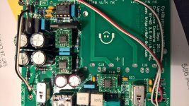
Hi,
I hope this is the right spot to ask for some guidance.
I recently bought a O2 & ODAC diy kit. I managed to assemble it, and it did work.
I then proceeded to resolder MOSFET Q2, because I could not put it in the case.
Something went wrong, I had to order a new MOSFET, installed it today but it wont work.
When i turn the O2 on, i hear a very loud unpleasant "flap" sound. I think i managed to create a short while soldering, there were some sparks. I guess I should have waited for the capacitors to empty their charge. Stupid me.
How do i proceed?
I have no idea if i killed some capacitors, should i buy a new kit (only the party and a new board, so i could be worse), or is there a commom fault that causes this"interesting" noise? For example only the ICs?
Some information, this was my first soldering project from scratch (an empty PCB). I do have a digital multimeter and could take some measurements or record the sound, I just did not want to leave my circuit on for any longer.
Any help is appreciated, Christian .
Last edited:
Hi again and thanks for welcoming me!
Good idea, so i got to the following step "Briefly Check The Supply Voltages", everything prior worked well.
I measured twice, the first time i got between 1 and3 Volts across BT1 positive and BT2 negative (i think i measured the right thing), the second time i got nothing.
Did not want to reinstall the ICs and potentially damaging them, so I did not continue with the guide.
- Home
- Amplifiers
- Headphone Systems
- The Objective2 (O2) Headphone Amp DIY Project