Been running my O2 for a while now, and everything seems to be working fine and all measurements came out correctly.
Yet today I ran my batteries flat for the first time and I heard some extremely loud popping which I can only figure being it power cycling I have the revised board with the lower ohm Resistors, so I assume this modification hasn't helped.
Could someone offer me some advice on how to fix this, it was rather loud, far louder than power on/off transients, I'm worried it could ruin my headphones.
Thanks.
Turn off the O2 and recharge the batteries.
No I'm just going to keep listening to the loud popping and hopefully ruin my headphones...
Seriously, is there no way to make it power off properly?
O2 unstable with weak battery
>>I ran my batteries flat for the first time and I heard some extremely loud popping
Replace the fixed 12v regulators with something like LM317. Build circuit like "remote shutoff" in the datasheet example and then add a comparator to that. When batteries drop assert the remote shutoff. You might also need a relay so that "off" latches somehow.
Could someone offer me some advice on how to fix this, it was rather loud, far louder than power on/off transients, I'm worried it could ruin my headphones.
If anyone would like to test a "fix", swap R9 for a 30k resistor and R25 for a 620k. You can do it without removing the existing resistors by just soldering a 1.0 meg ohm resistor across the existing 1.5 meg R25 on the back of the PC board, then solder a 330k resistor across the existing 33k R9 on the back of the board.
Use 1% resistors, or if using 5% test a bunch of them with DMM to find a couple close to the real value. Wattage doesn't matter for this, anything that fits works.
What you are doing is raising the voltage the batteries have to rise up to on their own again, once the O2 power management circuit turns off, to 1.35Vdc per cell or 9.45Vdc per battery, above the nominal 1.2Vdc but still less than the 1.45Vdc per cell or 10.15Vdc fully charged level.
The change should stop the oscillation entirely when the PM circuit shuts down, or at least slow the period way down.
Last edited:
Been running my O2 for a while now, and everything seems to be working fine and all measurements came out correctly.
Yet today I ran my batteries flat for the first time and I heard some extremely loud popping which I can only figure being it power cycling I have the revised board with the lower ohm Resistors, so I assume this modification hasn't helped.
Could someone offer me some advice on how to fix this, it was rather loud, far louder than power on/off transients, I'm worried it could ruin my headphones.
Thanks.
Curious on how many people have experienced this same issue. Mine's a recent build by JDSlabs, I'm using some t50rp's and vintage ortho's which are f-ing indestructible but if I had some sensitive IEM's I'd definetly be concerned about it damaging them. only happens maybe 2% of the time to me after the batteries drain though.
Hello!
I am very interested in what is your opinion about changing:
-NJM4556AD to LME49720HA (TO99 package, better sound than NA, MA package)
-NJM2068D to OPA1612AID.
Anyone has tried these opamps in The Objective2 ?
pls read this first NwAvGuy: Op Amps: Myths & Facts
Just checking in to see if anyone has heard from RocketScientist lately? He hasn't posted on his blog comments for a long time either.
Anyone? Is NwAvGuy OK?
Need Some Pro Help!
So I have completed my O2 build and while it looks great, only the left channel is working as intended.
I have completed all documented troubleshooting steps and now need some pro advice! Details below:
Since the left channel works perfectly, and there is no sound at all from right channel (no noise either) I can attest the power circuit is functioning properly, so its neither the FETs or regulators. I have reflowed every joint on the board to ensure there are no cold solder joints. All voltage and resistance tests are within range.
I have swapped U3 and U4 and still the problem persists in the right channel so both op-amps are functioning properly and the issue must be with the right channel output circuit? I discovered the 2068D was getting hot quickly when turned on. This is only happening when the 2068D right channel is being connected to its output channel circuit (I have a ALPS pot with a built in switch, and the 2068D does not get hot when powered on but the volme pot is turned off.) Thinking it might be a problem with one half of the 2068D op-amp, I put the DIP8 package on a protoboard and was able to use the "right" channel of the 2068D to drive the left channel of the O2 properly, yet the known working "left" side op-amp on the 2068D will not drive the right output channel in the same fashion.
Someone who knows more than me please help!
Thanks in advanced to such an awesome community and project!
(I have a ALPS pot with a built in switch, and the 2068D does not get hot when powered on but the volme pot is turned off.)
I'll take a guess that you didn't cut the switch leads off the pot+switch before you soldered it in, and that your pot+switch might be the ALPS RK0971221Z05? If so then when you turn on the switch on the pot it is shorting pin 1 of your NJM2608 to ground, which will short out the right channel (ring on the output TRS connector) and cause the chip to heat up (probably damaged).
As luck would have it, those two rear switch leads on the pot just fit right into the holes for the back gang of the 20mm version of the pot, which are pin 1 on one side and ground on the other. Unsoldering the pot may be difficult though.
If this is what happened, try to unsolder the pot and cut those switch leads off, then solder it back in, making sure the switch leads don't touch any pads.
Last edited:
15mm ALPS pot with switch warning
Agdr, that is the exact ALPS part I have and precisely what has occurred! I will have to wait until I get home this evening to unsolder and trim the rear pot switch pins, but looking at the pinout (which I previously assumed was the same) pin 1 is grounding out the right channel. Since the "right" channel of the 2068D is working to drive the "left" output channel in my testing, I am hoping the 2068D is not damaged.
Thank you so much for your quick response! I cant tell you how frustrating the weekend was while troubleshooting and every published test was coming out as expected.
That 15mm ALPS pot with switch does fit almost perfectly in the 20mm footprint and should be noted for others in the future since I ordered RK0971221Z05 because the official BOM part was unavilable.
I'll take a guess that you didn't cut the switch leads off the pot+switch before you soldered it in, and that your pot+switch might be the ALPS RK0971221Z05?
Agdr, that is the exact ALPS part I have and precisely what has occurred! I will have to wait until I get home this evening to unsolder and trim the rear pot switch pins, but looking at the pinout (which I previously assumed was the same) pin 1 is grounding out the right channel. Since the "right" channel of the 2068D is working to drive the "left" output channel in my testing, I am hoping the 2068D is not damaged.
Thank you so much for your quick response! I cant tell you how frustrating the weekend was while troubleshooting and every published test was coming out as expected.
That 15mm ALPS pot with switch does fit almost perfectly in the 20mm footprint and should be noted for others in the future since I ordered RK0971221Z05 because the official BOM part was unavilable.
Agdr, that is the exact ALPS part I have and precisely what has occurred!
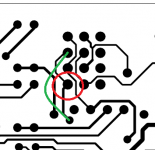
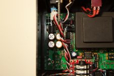
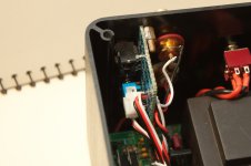
Well here is some good news, in the attachment below. You can just cut the two PCB traces on the bottom of the board going to one of the switch contacts, in that red circle below, with an xacto knife. Then jumper around the cut with an insulated wire following the green connection. That will disconnect the switch part of the pot and allow the signals to get where they are going without having to unsolder anything. That bottom connection on the green path is a via hole with no wire through it. That is OK, just put a little solder on it and solder the end of the wire right to the via.
The NJM2068 may seem to work OK after the fix, but the data sheet doesn't show any on-chip current limiting. The chip is probably damaged to some extent. Probably will be noiser, more distortion, etc. in that channel. Would be worth changing it next time you have a chance to order stuff.
Yes, you are probably the first one to discover this O2 layout hiccup!
I hadn't noticed that the 15mm pot + switch would just happen to fit into the hole pattern until your post. I'll bet RocketScientist didn't notice it either, lol. Originally there were just two rows of pot holes in the back section for the 20mm alps pot. But then Mouser ran out of them early on forcing RocketScientist to do a board re-work and add the two rows of holes in front for the 15mm pot. But in the process he apparently accidentally laid out the perfect hole pattern for a 15mm pot + switch. Attachments
Last edited:
Thanks Agdr!
I feel so lucky being the first one to find a new way to fail! But thanks so much for your help Agdr! The re-route sounds much easier than trying to desolder the pot pins with the package being completely flush on top. I will attempt the fix you mentioned tonight and cross my fingers that the 2068D is not damaged, but since its a relatively cheap component like the rest of this board, no worries if it is!
I have to say, I have read most of this ~3000 post thread and the level of support on this forum and site (especially for an open-source project) is amazing and please keep it up!
Well here is some good news, in the attachment below. You can just cut the two PCB traces on the bottom of the board going to one of the switch contacts, in that red circle below, with an xacto knife. Then jumper around the cut with an insulated wire following the green connection.
I feel so lucky being the first one to find a new way to fail!
But thanks so much for your help Agdr! The re-route sounds much easier than trying to desolder the pot pins with the package being completely flush on top. I will attempt the fix you mentioned tonight and cross my fingers that the 2068D is not damaged, but since its a relatively cheap component like the rest of this board, no worries if it is!I have to say, I have read most of this ~3000 post thread and the level of support on this forum and site (especially for an open-source project) is amazing and please keep it up!
Fixed!
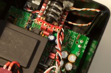
I just wanted to update and say the reroute fix worked perfectly. I have attached a pic just in case it can help someone in the future. Also the 2068D is not noticeably damaged (no noise etc) perhaps because I never stay on for more than a few seconds or let it breach 200F when testing the short.
Thanks again Agdr!
You can just cut the two PCB traces on the bottom of the board going to one of the switch contacts, in that red circle below, with an xacto knife. Then jumper around the cut with an insulated wire following the green connection.
I just wanted to update and say the reroute fix worked perfectly. I have attached a pic just in case it can help someone in the future. Also the 2068D is not noticeably damaged (no noise etc) perhaps because I never stay on for more than a few seconds or let it breach 200F when testing the short.
Thanks again Agdr!
Attachments
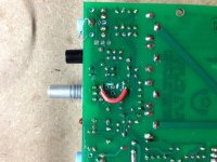
I just wanted to update and say the reroute fix worked perfectly.
I'm glad that worked out!
hey guys
first,thanks RocketScientist,
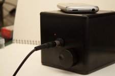
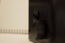
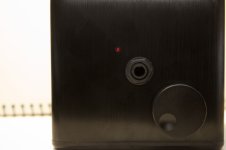
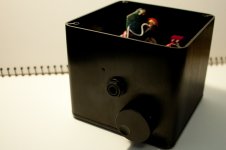
this is my O2 Black Cube version
just finish this little thing about 1 hour ago
it's a desktop only version,the black case come from a 110mm*110mm*100mm transformer cover, perfectly fit!
first,thanks RocketScientist,
this is my O2 Black Cube version
just finish this little thing about 1 hour ago
it's a desktop only version,the black case come from a 110mm*110mm*100mm transformer cover
, perfectly fit!Attachments
Last edited:
link??
thermal distortion was recognized, minimized by design, layout in op amp chips long ago
you can often see some evidence of the residual of this type of distortion in comprehensive THD, IMD plots
it can be further (meaninglessly for audible perception) be reduced by using composite multiloop circuits with the output op amp in the global loop of a input op amp which can be operated from subregulated, reduced power supply – the input device power only varies by uW
- Home
- Amplifiers
- Headphone Systems
- The Objective2 (O2) Headphone Amp DIY Project