No, the 7812 voltage reg, that's U5.
Thanks for clarification. Just to double-check - all those measurements are without U5 (or any other U except U2) installed?
Thanks for clarification. Just to double-check - all those measurements are without U5 (or any other U except U2) installed?
Having no 12 volts is a problem right at the front end and so you can leave the other parts in place. Just set the power switch S1 to off which will isolate the circuitry anyway.
My O2 has become problematic after a couple of years with no issues... I've followed the troubleshooting guide on NwAvGuy's website and have found the problem in the negative power supply - I measure -25V on the non-striped end of D4, but then 0V on the non-striped end of D5.
Tracing back through the circuit I also measure 0V on the IN leg of U6 which seems wrong... It seems like the only way this could happen is if there's a break in the trace in the circuit board between D4 and U6. Should I just run a wire or something?
Thanks
Tracing back through the circuit I also measure 0V on the IN leg of U6 which seems wrong... It seems like the only way this could happen is if there's a break in the trace in the circuit board between D4 and U6. Should I just run a wire or something?
Thanks
Its 2 years since he last logged on.
That's quite a while.
Doh! One of big condensator legs were not soldered - as soon as I've spotted it I've covered myself with facepalms: how the hell can I miss such a big and obvious glitch?!
Fixing that gave proper readings for D1, D5 but now there's another problem:
U2 (installed), U3 (not installed) and Q1 (via R24) give unexpectedly low voltage, something in the order of 0.4V where 11V is expected.
The top row of U2 pins (if we look at it the same way it's shown in troubleshooting checklist) are measuread as
-10.6V -0.42V -9.4V while expected values are 9.8V -11.8V -10V
The botom row correspondingly:
-0.4V -9.6V -9.0V -10.7V with expected -11.7V -8.4V -10V -11.8V
The expected 9.8V pin is marked as (Q2 gate) in measurements picture so I'm not sure if I'm measuring it properly - reversed voltage sign looks especially weird in here.
The same concern is for -11.4V end of R24 which is marked as (Q1 gate) and gives me -0.4 when measured relative to the ground.
Could you help me with further troubleshooting?
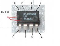
Its easier to follow if you can quote pin numbers and voltages ") All 8 legged IC's follow the same pattern as shown in the picture.
All 8 legged IC's follow the same pattern as shown in the picture.
So with your meter (black lead) on ground, what is the voltage on,
Pin 8. It should be around 11 to 12 volts.
Pin 4. It should be around minus 11 to 12 volts.
They are the supplies to the opamp.
Now record the voltages on the other pins and report back with the results.
Pin 1 = ?
Pin 2 = ?
Pin 3 = ?
Pin 5 = ?
Pin 6 = ?
Pin 7 = ?
Report your readings and we'll see whats what.
All 8 legged IC's follow the same pattern as shown in the picture. So with your meter (black lead) on ground, what is the voltage on,
Pin 8. It should be around 11 to 12 volts.
Pin 4. It should be around minus 11 to 12 volts.
They are the supplies to the opamp.
Now record the voltages on the other pins and report back with the results.
Pin 1 = ?
Pin 2 = ?
Pin 3 = ?
Pin 5 = ?
Pin 6 = ?
Pin 7 = ?
Report your readings and we'll see whats what.
Without being overly familiar with the intricacies of the power management circuits, I'd say it shouldn't matter that much. The worst that could happen would be more power-on pop noise. A plain MC7912CT would be fairly old stock though, only CTGs are still in production.
It's odd how negative reg failures seem to occur fairly regularly. Maybe another protection diode would have been useful? Has anyone ever looked at what's going on during power-up/down at the regs with a scope?
It's odd how negative reg failures seem to occur fairly regularly. Maybe another protection diode would have been useful? Has anyone ever looked at what's going on during power-up/down at the regs with a scope?
Reconnected the trace with a wire and the 7912 has 4V on the out leg so I guess I need to replace it - I can get a 7912CT much more easily than a 7912ACTG. The difference is from 2% to 4% tolerance - is that going to matter in this situation?
It won't matter at all.
(I take it you still only have four volts on the reg even when the switch S1 is off. If there were a short on the main circuitry it could drag things down but then you would find things getting hot. If the switch is off and there is 15 or more going in and less than 12 coming out then the reg is duff)
Ok, I've made U2 measurements according to piout:
1: -0.46V (-11.7V)
2: -9.95V (-8.4V)
3: -9.4V (-10V)
4: -11.15V (-11.8V)
5: -9.48V (-10V)
6: -0.475V (-11.8V)
7: -11.2V (9.8V)
8: -0.49V
That's with only U2 installed, no batteries and AC power on - if I turn off S1 all the values drop to -0.014..-0.046V
The values in brackets are taken from official troubleshooting guide.
I'm especially puzzled by lack of voltage at pin1 and reversed voltage at pin7 - could it be fried U2 or some soldering mistake?
Your main problem is pin 8. That is the positive supply to the chip and should be at +12 volts. The positive rail is missing and is why everything appears to be a negative voltage. Look at the circuit and it will make sense.
You need to backtrack and check the voltage firstly at the 7812 input which should be 15volts or more for the reg to work. The voltage on pin 3 (output) should be +12 volts. That voltage should also be present on both sides of D1. From there it goes via the switch to the main circuitry.
Just do those checks carefully
Is there somewhere that I can find a better layout drawing than the pdf on Nuwavguys blog post. I received a couple of boards many months ago from Qusp in Australia for my kids to build and now my daughter is building one of the boards. It isn't clear how the U2 and other transistors are supposed to be placed. No EBC designation I can see on that PDF. I don't think I want to read through the entire 400 pages of entries if someone can just point me in the right direction. Hopefully there aren't any major changes from the original bom? Anyone know what happened to Qusp, Jeremy, I lost contact with him and am curious what happened if anyone knows.
Thanks,
Steven
Just realized I was looking at a voltage regulator she was asking me about, duh. But still any better layout drawing than the original?
Thanks,
Steven
Just realized I was looking at a voltage regulator she was asking me about, duh. But still any better layout drawing than the original?
Last edited:
I don't know of any better diagrams, in fact I've never delved beyond working just from the circuit diagram to answer the questions in this thread. U2 should be easy to ID. Just trace the rails to pins 4 and 8. If you pull up the data sheet for the FET's then they can be fitted by a similar method. Trace the incoming supply to ID the "source" pin.
Qusp... now you mention it, no, haven't noticed him around for a while. Over 2 months since last log-in.
Qusp... now you mention it, no, haven't noticed him around for a while. Over 2 months since last log-in.
The component placement and orientation is clearly shown on NwAvGuy's PDF and on the silkscreen of the board, no need to look at schematics or trace any pins...
The only change from the BOM in the PDF is that two of the 220nf film caps have been changed to 1uF MLCs. (The ones at the voltage regs)
The only change from the BOM in the PDF is that two of the 220nf film caps have been changed to 1uF MLCs. (The ones at the voltage regs)
- Home
- Amplifiers
- Headphone Systems
- The Objective2 (O2) Headphone Amp DIY Project