A third channel might be interesting to at least test. I know the M³ Headphone Amplifier ) uses one and it seems to measure well and has a loyal following.RocketScientist, how about adding a third channel (a copy of the L/R channel, with unity gain) to create a 3-channel headphone amp?
The 3-channel topology keeps headphone return currents from disturbing the signal ground.
Btw, count me in as interested.
My personal belief is with proper PCB layout and grounding you shouldn't need a third channel. If a 200 watt power amp with ground currents 100 times higher can have really low distortion, it's comparatively easy to manage the ground currents in a headphone amp.
Some claim a third channel also provides a more "symmetrical" drive for the headphones, lowers crosstalk, etc. But I haven't seen any proof of those supposed benefits. There's also a downside. In terms of noise performance a 3 channel amp will potentially be worse. It's also significantly less efficient, produces more heat, costs more, requires a bigger PCB, and potentially a bigger enclosure.
It would be fun to test the claims but I'm curious what others think? Is it worth testing? It might be possible to have an optional 3rd channel on a PCB that was about 50% larger with some jumpers, etc.
Or I could possibly provide some pads/jumpers on a 2 channel PCB making it easy to use a 2nd PCB only half populated as a ground channel. But that might somewhat compromise the grounding layout.
Ultimately, the effects of ground currents, crosstalk, etc, are measurable. So the Prism dScope could help make the choice easier. Does anyone know if there are comparable measurements anywhere for a 2 ch vs 3 ch design?
I've explained the engineering analysis of "3-channel" amplifiers as advocated by some at Head-Fi in several posts there - I have given reasons that the claimed "advantages" don't work as advertised
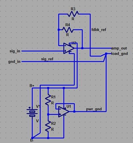
there is a distinction between "3-channel" and "active gnd" - "active gnd" is sometimes used to split a single supply such a a battery or wall wart - but proper wiring connects input signal gnd and load gnd together for fewer introduced errors than the "3-channel" scheme
I would go for 4-pin heaqphone cable connectors, separating R/L load gnd paths (TRS "single point" contact can have 10 mOhm common gnd R in the jack/plug interface)
dual polarity supply, then "dual mono" and/or bridged/balanced output for real engineering advantages in an "ultimate" headphone amp
the BUF and LME (and TPA6120 - I don't know why peole get stuck on only condidering unity gain buffers in the loop) are so good that full Class A output operation is probably of no audible advantage but it does ease the layout considerations of keeping the "half-wave" Class AB +,- supply currents from giving some nonlinear common impedance couping on the board
I've also shown how to bias op amps for Class A output when they can handle the heat
http://www.diyaudio.com/forums/soli...ain-composite-op-amp-circuits.html#post951118
http://www.head-fi.org/forum/thread/188758/ad8397-class-a/15
at one Head-Fi gathering some who swore they could hear differences in op amps couldn't tell when my parallel TPA6120 output amp was biased Class A at ~220 mA vs the few mA when the bias V was turned off
there is a distinction between "3-channel" and "active gnd" - "active gnd" is sometimes used to split a single supply such a a battery or wall wart - but proper wiring connects input signal gnd and load gnd together for fewer introduced errors than the "3-channel" scheme
The Pimeta’s "3-channel" topology is fundamentally flawed - most technical reasons given for it are simply not true or can be bettered by proper layout
"active supply splitter" can be useful when wanting to use single V supply - the single active gnd should be used for input, feedback and load gnd
but "3-channel" puts the gnd “buffer” amp in series with the load - with the input and feedback grounds separated from the load gnd - this means all of the error of the "output gnd" buffer is in series with the headphones - giving distortion and "output gnd" impedance crosstalk that is worse than with a good "passive" gnd of heavy conductor with signal input gnd, feedback gnd "star" connected with the load common ground pin of the TRS connector
A "active gnd" showing star at output - can better "3-channel" performance:
...
I would go for 4-pin heaqphone cable connectors, separating R/L load gnd paths (TRS "single point" contact can have 10 mOhm common gnd R in the jack/plug interface)
dual polarity supply, then "dual mono" and/or bridged/balanced output for real engineering advantages in an "ultimate" headphone amp
the BUF and LME (and TPA6120 - I don't know why peole get stuck on only condidering unity gain buffers in the loop) are so good that full Class A output operation is probably of no audible advantage but it does ease the layout considerations of keeping the "half-wave" Class AB +,- supply currents from giving some nonlinear common impedance couping on the board
I've also shown how to bias op amps for Class A output when they can handle the heat
http://www.diyaudio.com/forums/soli...ain-composite-op-amp-circuits.html#post951118
http://www.head-fi.org/forum/thread/188758/ad8397-class-a/15
at one Head-Fi gathering some who swore they could hear differences in op amps couldn't tell when my parallel TPA6120 output amp was biased Class A at ~220 mA vs the few mA when the bias V was turned off
Last edited:
Thanks JCX. That pretty much sums up most of my thoughts on a third channel. But I was trying to keep an open mind and/or wondered if I might be missing something.
I'm all for innovation and creativity but analog class A/B audio amplifier design is relatively mature. Lots of things have been tried over many decades but few gain long term traction. Once we achieved sufficient speed, linearity, bandwidth and direct coupling, the rest has mostl been refinement of already well proven conventional circuit topologies and the semiconductors themselves.
There have been various fancy bias schemes alleging Class-A performance with Class AB efficiency, "smart" (switched multi-rail, etc.) power supplies, "diamond bridge" distortion canceling circuits, MOSFET outputs, feed-forward, low TIM designs, IGBT's, and many more new twists. But surprisingly few of these "innovations" stayed around and/or ever gained much acceptance. Many remind me of the 100 MPG carburetors and other things that were supposed to magically quadruple the efficiency of internal combustion engines but never seemed to survive any sort of objective testing.
Is there a preferred PCB mount 4 pin headphone connector? Assuming there's enough room along one edge, it would be easy to provide for that. I was already thinking of both 1/4" and 3.5mm to avoid external adapters.
Does anyone have thoughts regarding the power supply alternatives on the previous page?
I would probably cast a vote for option #2 for the PS, include something on the board with the option of not populating it and instead using something external.
I had mentioned a Jung SR or clone in that "wire" thread, but there are so many good supplies out there and everyone has their favorite. I'm building up an AMB Sigma22 right now for another project that I may wind up re-purposing for this board.
Just my two cents.")
I had mentioned a Jung SR or clone in that "wire" thread, but there are so many good supplies out there and everyone has their favorite. I'm building up an AMB Sigma22 right now for another project that I may wind up re-purposing for this board.
Just my two cents.
A third channel might be interesting to at least test. I know the M³ Headphone Amplifier ) uses one and it seems to measure well and has a loyal following.
My personal belief is with proper PCB layout and grounding you shouldn't need a third channel. If a 200 watt power amp with ground currents 100 times higher can have really low distortion, it's comparatively easy to manage the ground currents in a headphone amp.
Some claim a third channel also provides a more "symmetrical" drive for the headphones, lowers crosstalk, etc. But I haven't seen any proof of those supposed benefits. There's also a downside. In terms of noise performance a 3 channel amp will potentially be worse. It's also significantly less efficient, produces more heat, costs more, requires a bigger PCB, and potentially a bigger enclosure.
It would be fun to test the claims but I'm curious what others think? Is it worth testing? It might be possible to have an optional 3rd channel on a PCB that was about 50% larger with some jumpers, etc.
Or I could possibly provide some pads/jumpers on a 2 channel PCB making it easy to use a 2nd PCB only half populated as a ground channel. But that might somewhat compromise the grounding layout.
Ultimately, the effects of ground currents, crosstalk, etc, are measurable. So the Prism dScope could help make the choice easier. Does anyone know if there are comparable measurements anywhere for a 2 ch vs 3 ch design?
Hi Rocketscientist,
I have an M3 and while it does some things really well, Im not sure I like it compared to my F4. But I really need more time with it before I make any decisions. But the reason Im posting here is I like the sound of your project and have always wondered about the ground channel. I personally would be interested in having one that can be be bypassed at the flick of a switch cos I cant see how they can possibly help, but then again Ive been wrong many times in audio.
Hello,
4 pin output preference? If the L&R grounds are separate that means that 99 + % of the stock headphones will need to be rewired. My preference would be a mini 4-pin XLR.
Power supply preference is flexibility. The Op-Amps offer high PSRR to start with and 317 / 1085 type regulator will work well however others prefer dark as the night shunt regulators. I like gel cells for this type of application.
DT
All just for fun!
another point for using a CFA with gain as the outupt buffer is that you can then subregulate the input op amp ps withou losing any Vswing at the output - the sub regualtion is much more effective because the input op amp doesn't have any significant dynamic current demand
since the op amp psrr is the op amp excess loop gain you get ridiculus psrr in the composite amp
since the op amp psrr is the op amp excess loop gain you get ridiculus psrr in the composite amp
Yes, good point. Perhaps I should include jumper pads and an easy to cut trace in the power supply rails between the gain and output stage? That would allow someone to easily split the supplies as you suggest. Because of the high PSRR it's likely overkill, but some like overkillanother point for using a CFA with gain as the outupt buffer is that you can then subregulate the input op amp ps withou losing any Vswing at the output - the sub regualtion is much more effective because the input op amp doesn't have any significant dynamic current demand
since the op amp psrr is the op amp excess loop gain you get ridiculus psrr in the composite amp
In a big audio power amp you want the output stage to swing as close to the rails as possible for maximum efficiency. So having either gain in the output stage, or higher rails for the earlier stages is a very good idea. But, in a headphone amp, burning a few more tenths of a watt in the output stage isn't a big dea. And, with 15 volt rails, there's more output swing than I can imagine just about anyone needing.
I know you're a huge fan of the TP6120 and it looks to be an impressive part. But I have one serious reservation. TI says it may need to dissipate upwards of 2 watts of power. And DIY'ers don't have any good way to properly solder the "hidden" heatsink pad underneath the device without reflow equipment and solder paste. So it's much less DIY-friendly compared to the simple 5 pin tabbed package of the LME49600.
I realize you came up with a solution to this problem mounting the parts upside down, re-bending the pins, etc., but it's not a very practical DIY solution for most. My goal is a relatively low cost, simple, easy to build solution with world class performance. So elaborate heat sinks, mechanical work, and/or tricky soldering are not ideal.
If I thought the TP6120 would yield significantly better performance I'd be more open to it. But I'm not sure it will? It has higher peak current capability, and can have gain, but do you think it would yield lower overall total distortion than the LME49600 design?
... My goal is a relatively low cost, simple, easy to build solution with world class performance. ...
That's my type of project
with added gain in the loop there is "extra" distortion reduction
there is no chance that the output stage will limit the performance with the TPA6120 in a multiloop - just look at the distortion spec when operating by itself, providing all of the loop gain
the LME49600 distortion # is for the buffer operating inside the LME49710 55 MHz GBW feedback loop
apply the same factor of excess loop gain for all audio frequencies to the TPA6120 distortion plots and the output distortion will not be measurable
since the LME47910/4562 is nearly a pure integrator just divide the 55 MHz GBW product by frequency and by amplifier closed loop gain to get the excess loop gain (or feedback factor) output stage distortion reduction at any frequency
for Av 10, 1KHz the output distortion is reduced by ~5000x
but you can also add loop gain with the TPA6120 unlike a buffer - use modified integrator feedback around the TPA6120 so its gain can be >100x over all audio frequencies
then the input op amp then only swings ~ 100 mV at audio frequencies
2nd order distortion decreases in percentage 1:1 with level, third order by the square of level - higher order distortions follow the n-1 power law too so they disappear even more quickly
so with added loop gain from the TPA6120 the input op amp is operating at >100x increased linearity due to the reduced signal level it has to provide - this is in addition to the ~1/F reduction in output stage distortion which doesn't "care" where in the loop the excess gain is distributed
as for heat sinking the TPA6120 should do ~ 1W without the power pad connection - quite enough in Class AB if you've managed to coordinate your ps V and load for most headphones
Perander's QRV07 project uses the TPA6120 - a power pad soldering comment is here: Re: TPA6120 headphone amplifier power supply capacitance for the output THD specified - Audio Amplifiers Forum - Audio Amplifiers - TI E2E Community
I would try using one large hole instead of the via grid for hand soldering - say ~ 1/2 the area of the power pad - then you can get solder, soldering iron tip in the hole from the backside
for just 1 or 2 TPA the upside down approach could use much smaller video chip coolers - a spring clip giving a clamping force of ~20x the weight of the tiny Al heatsink shouldn't bend the pcb out of shape
Last edited:
jcx, I'm talking about overall distortion performance of the pure National reference design with global feedback, vs the TPA6120 in either global or multi-loop feedback. I honestly don't think the TPA6120 in the real world will outperform the National design in any measurable way beyond higher current capability which is solved with parallel LME buffers. Do you agree with that? Others, such as Doug Self, have conducted real world testing and concluded the National LME49xxx audio parts measure the best in real world applications--better than those from Analog Devices, Linear Tech, and Burr Brown/TI.
Again, the goals include one-size-fits-nearly-all and being as easy to build as possible. I still think trying to properly mount the TPA6120 is a significantly greater challenge than the 5 pin tabbed LME49600. Yes you could lower the supply rails for low impedance headphones reducing dissipation, but what if someone wants to use both low and high impedance inefficient cans?
Yes, you could try to heat a blob of solder on the pad from the underside of the board using vias, but I'm guessing with all that copper area it's not going to work. The unmelted residual solder on the pad is going to keep the TPA6120 up off the pad. And you're not going to melt all of it using a single soldering iron on a single via below the part. So, at best, you'll melt a local area above the via and the rest of the unmelted solder will keep the part from "settling down" as it needs to. And this would also interfere with soldering the signal and power pins as the part won't sit flat on the board with solid uneven solder trapped underneath it.
If you want to apply all the solder from the bottom, you can have vias as large as the PCB vendor will allow for drilled plated through holes. That varies from vendor to vendor but it's usually around 5 mm (.19 in) diameter or less. You might be able to get a soldering iron tip and solder through such a hole and try to wick some solder underneath, while somehow holding the part in precise alignment and flat to the board. And if you used more than one such via to try and solder most of the pad, once you soldered the second via, the part would likely never move again, and would also be very difficult to remove from the PCB if it failed, damaged or was mis-aligned. And it's still blind and you don't really know how much of the pad is really soldered.
And someone might easily overheat the TPA6120 trying to get the pad properly soldered. And that could change its performance in non-obvious ways. Infrared reflow evens follow precise temp ramps and heating time profiles to avoid silicon damage. You can't do that at home with a soldering iron. Yeah it might work OK, but it's more Rube Goldberg and more of a DIY challenge than the LME part. And I'm not still not clear why the trade off is worthwhile?
If this was a commercial design with nearly all SMT parts being assembled on a pick/place/reflow line I would be much more open to the TPA6120. Perhaps that could be a different project if there's enough interest? Right now I'm just trying for great measured performance in as low cost and DIY-friendly of design as possible. And then see how the low-distortion design compares to a single op amp cmoy-like design and a discrete class-A amp. Once the results of the comparison are published the next step will hopefully be more clear.
Last edited:
Hello,
This heat thing need not be a big issue. First considering the buffer “sink” being soldered to the board is beyond the comfort level of many DIYer’s. it need not be but it is.
My preference is the 5 legged bug. Attach a heat sink if needed.
The longer version; the quantity of heat can be calculated. The Buffer has a BW pin if it is shunted the buffer will draw a known current. Multiply the current times the voltage to one rail and get watts. Watts times 3.41 gives BTU’s blah blah blah. When I built one of these things point to point bird nest style using a 5 pin BUF 634 the die did not get hot to the touch. No heat sink was required.
12 * 0.015 = 0.18 watts, less than the heat from a ¼ watt reisitor.
I recommend that you mock-up a couple versions to see what is buildable and see how hot things get.
DT
All just for fun!
I had though your earlier question was straight - not rhetorical
In a word No - I am still allowing for using the LME49710 as input op amp but I thought I was pretty clear on how added loop gain from a CFA output op amp can improve the linearity of the input/global loop feedback op amp
to appeal to the LME part's "reputation" is not engineering - feedback amplifiers do work as I explained and you can better the performance of the LME49600 example circuit - I pointed to the numbers you need to show the TPA6120's 32 Ohm load distortion is expected to be ~5000x less than the graph numbers - way better than the unity buffer circuit's (1 kHz) number
the application circuit is fine, I seriously doubt any DBT test will let you tell the difference but if the question is can the measured distortion be bettered with added gain in the loop then you need to understand distortion and feedback at the level explained in Cherry’s last JAES paper: Cherry, “Estimates of Nonlinear Distortion in Feedback Amplifiers” JAES V48#4 2000
I have made indirect measurements of advanced multiloop with gain in the output stage circuits where the IMD distortion was below the ~160 dB resolution of my -130 dB spot noise soundcard and added 30 dB error amplification gain stage
you can build a fine amp either way - the output distortion will not be the limting factor - for noninverting gain circuits the input stage common mode nonlinearity is bigger with real world input Z, feedback Z mismatch - "reasonable" volume pot source resistance varies KOhm over the setting range
pcb manufacturers will happily plate any hole you want to drill - think through hole parts, even heatsink mounting pins can be soldered, board mounting holes are plated unless you drill out after plating
there may be limitations on how big a hole they want to "tent" with solder mask - in wave soldering there is a max dia without tenting to prevent the wave from flooding the board
Peranders TPA6120 board clearly doesn't solder mask the power pad pattern backside - for stencil/paste/reflow you don't want the holes open because wicking will starve the joint - for hand assembly you can just feed solder until the holes fill/and use solderwick to mop up any excess while keeping generous fillets
...If I thought the TP6120 would yield significantly better performance I'd be more open to it. But I'm not sure it will? It has higher peak current capability, and can have gain, but do you think it would yield lower overall total distortion than the LME49600 design?
jcx, I'm talking about overall distortion performance of the pure National reference design with global feedback, vs the TPA6120 in either global or multi-loop feedback. I honestly don't think the TPA6120 in the real world will outperform the National design in any measurable way beyond higher current capability which is solved with parallel LME buffers. Do you agree with that? ...
In a word No - I am still allowing for using the LME49710 as input op amp but I thought I was pretty clear on how added loop gain from a CFA output op amp can improve the linearity of the input/global loop feedback op amp
to appeal to the LME part's "reputation" is not engineering - feedback amplifiers do work as I explained and you can better the performance of the LME49600 example circuit - I pointed to the numbers you need to show the TPA6120's 32 Ohm load distortion is expected to be ~5000x less than the graph numbers - way better than the unity buffer circuit's (1 kHz) number
the application circuit is fine, I seriously doubt any DBT test will let you tell the difference but if the question is can the measured distortion be bettered with added gain in the loop then you need to understand distortion and feedback at the level explained in Cherry’s last JAES paper: Cherry, “Estimates of Nonlinear Distortion in Feedback Amplifiers” JAES V48#4 2000
I have made indirect measurements of advanced multiloop with gain in the output stage circuits where the IMD distortion was below the ~160 dB resolution of my -130 dB spot noise soundcard and added 30 dB error amplification gain stage
you can build a fine amp either way - the output distortion will not be the limting factor - for noninverting gain circuits the input stage common mode nonlinearity is bigger with real world input Z, feedback Z mismatch - "reasonable" volume pot source resistance varies KOhm over the setting range
pcb manufacturers will happily plate any hole you want to drill - think through hole parts, even heatsink mounting pins can be soldered, board mounting holes are plated unless you drill out after plating
there may be limitations on how big a hole they want to "tent" with solder mask - in wave soldering there is a max dia without tenting to prevent the wave from flooding the board
Peranders TPA6120 board clearly doesn't solder mask the power pad pattern backside - for stencil/paste/reflow you don't want the holes open because wicking will starve the joint - for hand assembly you can just feed solder until the holes fill/and use solderwick to mop up any excess while keeping generous fillets
Last edited:
I figured if there were a whole bunch of takers for the nearly entirely surface mount "Wire" version, just one big SMT part with only a few pins is child's play by comparison.Hello,
This heat thing need not be a big issue. First considering the buffer “sink” being soldered to the board is beyond the comfort level of many DIYer’s. it need not be but it is.
If I include the pins for the TI BUF634 version, then it can be entirely through hole. You just can't use the LME49600.My preference is the 5 legged bug. Attach a heat sink if needed.
That just gets you the quiescent (idle) power. The real max dissipation is many times that driving low impedance inefficient headphones to loud levels. Class-AB audio amps are not very efficient when playing real music--especially if the supply rails are much higher than they need to be. The total power could approach 2 watts.The longer version; the quantity of heat can be calculated. The Buffer has a BW pin if it is shunted the buffer will draw a known current. Multiply the current times the voltage to one rail and get watts. Watts times 3.41 gives BTU’s blah blah blah. When I built one of these things point to point bird nest style using a 5 pin BUF 634 the die did not get hot to the touch. No heat sink was required. 12 * 0.015 = 0.18 watts, less than the heat from a ¼ watt reisitor.
The latest version of the NG98 uses the TPA6120
HA INFO Audio Electronics
Includes DAC, metal case, power adaptor and shipping for $99 on fleabay. I've been very happy with my (previous version) op amp + BUF634 NG98 in terms of build quality. After the discussion above you guys have me convinced to get one of these new ones too.
For this (first) board I would love to see the LME49720/LM4562 + LME49600/BUF634 board. But if a TPA6120 version is done that might be very interesting too. Probably a lot that could be improved DIY over commercial.
Last edited:
if I were tasked to create the lowest measureable distortion audio source with today's COTS technology I would consider the ESS Sabre DAC chips with composite op amp I/V direct to headphones
in virtual gnd/inverting mode as an I/V stage the common mode nonlinearity isn't an issue, "32 bit" digital volume control will beat any pot
in virtual gnd/inverting mode as an I/V stage the common mode nonlinearity isn't an issue, "32 bit" digital volume control will beat any pot
Last edited:
In a word No - I am still allowing for using the LME49710 as input op amp but I thought I was pretty clear on how added loop gain from a CFA output op amp can improve the linearity of the input/global loop feedback op amp
I think we may only differ regarding what determines the real world THD+N floor and hence the "weakest link". That's what I meant by "overall total distortion". If the THD+N components of the National design are already going to be close to the final overall noise floor, improving things further doesn't help the cause much. As you said the input volume control, for example, is likely to be a bigger limitation.
No argument there for a theoretical reduction.feedback amplifiers do work as I explained and you can better the performance of the LME49600 example circuit
I have made indirect measurements of advanced multiloop with gain in the output stage circuits where the IMD distortion was below the ~160 dB resolution of my -130 dB spot noise soundcard and added 30 dB error amplification gain stage
Good to know, and impressive. But, again, I'm talking about real world performance which includes a real world source and no "distortion magnifier" to artificially increase the dynamic measurement range. I suppose a case can be made for doing that, but that's more of a theoretical, not real world, advantage. It's hard enough to justify 0.001% THD+N as being audible let alone an order of magnitude or two lower.
The one area where a multi-loop design might do better is in differencing testing. You might get a slightly deeper null. But even then I'm skeptical as I suspect noise, phase shift, and other variables will still dominate.
Agreed.you can build a fine amp either way - the output distortion will not be the limting factor - for noninverting gain circuits the input stage common mode nonlinearity is bigger with real world input Z, feedback Z mismatch - "reasonable" volume pot source resistance varies KOhm over the setting range
Actually they're doing the drilling, and their drilling machines have a maximum CNC bit size without a human mounting something bigger. So when you buy prototype quantity PCBs you're stuck with a fixed "drill rack" unless you want to pay $500+ for a single board. And even if you pay extra for routed (versus drilled) holes, the "cheap" routing happens when the panels are cut apart which is after the plating process. If you want routing before plating that's an extra process and you pay dearly on low volume runs. So, depending on the vendor, the max drill size is usually in the 5mm - 6mm range. That's the biggest plated through hole you can get on a standard "economy" proto run that gets panelized with a bunch of other proto jobs.pcb manufacturers will happily plate any hole you want to drill - think through hole parts, even heatsink mounting pins can be soldered, board mounting holes are plated unless you drill out after plating
there may be limitations on how big a hole they want to "tent" with solder mask
You can try, but as I said, it's very much a blind operation. And, without x-ray at least, you really don't know how much of the pad you soldered. I work with assembly contractors all the time. And, despite all their expensive equipment, they hate concealed thermal pads when doing hand prototype assembly or rework. They usually won't guarantee either not damaging the part, and/or sufficient thermal conduction when doing hand assembly.for stencil/paste/reflow you don't want the holes open because wicking will starve the joint - for hand assembly you can just feed solder until the holes fill/and use solderwick to mop up any excess while keeping generous fillets.
And if the professionals that do it for a living and have all the right equipment are hesitant, I'm far more hesitant to propose it for a DIY solution for someone with a hobby iron. I have no doubt some have made it work, I'm just not comfortable with it. There's plenty to go wrong as it is without adding something even more difficult. If you read through the Wire thread there are multiple assembly issues, confusion over how to do things, etc. And that's typical in these projects. I'd rather make it easier, not harder.
As Dual Triode said, even the simple 5 pin DPAK might be a challenge for some. And using the LME49600 allows including pads for the BUF634 TO-220-5 version making the design completely through hole. That can't be done for a TPA6120 design.
If it turns out, after building and measuring, there's a need for even lower real world distortion than the National reference design can deliver, I'm open to the TPA6120, multi-loop feedback, etc. But, for now, it just doesn't seem like a worthwhile trade off. If others disagree, please feel free to join in here?
Thanks. I didn't realize you could buy a TPA6120 DAC for $99. I suspect it uses global feedback, not local/multi feedback as jcx has proposed. But it would at least be interesting to compare the peak current capabilities of the different devices and see how it measures up in other ways.The latest version of the NG98 uses the TPA6120.
Includes DAC, metal case, power adaptor and shipping for $99 on fleabay. I've been very happy with my (previous version) op amp + BUF634 NG98 in terms of build quality. After the discussion above you guys have me convinced to get one of these new ones too.
For this (first) board I would love to see the LME49720/LM4562 + LME49600/BUF634 board. But if a TPA6120 version is done that might be very interesting too. Probably a lot that could be improved DIY over commercial.
If you liked the earlier version perhaps it will be the exception to my rather disappointing experiences with eBay "audiophile" offerings that seem too good to be true (and usually have been). But, in fairness, most of those have been DIY boards rather than complete products.
As I said earlier, if the performance is unacceptable, at least the case could be re-used for a better DIY design.
I would be really curious to hear the difference between the NG98 (my BUF634 version) and the board proposed here, powered by a better PS, and driven by a better DAC board. Might not be any or it might be quite noticable! Either way, will be fun to try.
Yeah the TPA6120 design points that you and jcx have been pondering probably go way beyond whatever is being done in the new NG98.
Yeah the TPA6120 design points that you and jcx have been pondering probably go way beyond whatever is being done in the new NG98.
It would be interesting to compare them. Most of the eBay Asian audiophile DAC vendors are famous for either following the "trend of the month" and/or trying to offer something for everyone. Generally having a large number of products and/or frequently changing them to feature the latest chip means they probably don't spend a lot of time refining any one design.I would be really curious to hear the difference between the NG98 (my BUF634 version) and the board proposed here, powered by a better PS, and driven by a better DAC board. Might not be any or it might be quite noticable! Either way, will be fun to try.
Little Dot, for example, has about a dozen current DACs/headphone amps and that doesn't include all the previous mk-whatever versions they no longer make. Audio-GD has closer to two dozen.
HA Info (maker of the NG98) seems better than most in that regard. They only have 3 current DACs listed. But I do wonder why they switched from the BUF634 to the TPA6120? Was there a problem with the BUF634 version? Is the TPA6120 more "trendy" and they thought it would sell better? Did they do their own internal comparison and decided the TPA6120 performs and/or sounds better?
I think part of it is the same as with big audiophile companies anywhere--they simply are trying to differentiate their products from their competition. They also chase and copy each other. If Brand X comes out with a TPA6120 version to try and stand apart, Brand Y might feel they need to offer one too.
So, yes, it would be a very interesting comparison--both their measurements and also a blind ABX listening test.
- Status
- This old topic is closed. If you want to reopen this topic, contact a moderator using the "Report Post" button.
- Home
- Amplifiers
- Headphone Systems
- National LME49600 Reference Design Project