layout is good so far
alright, parts are starting to trickle in from mouser and digikey (the 2sk214's i ordered will probably be backordered through the new year, knowing my luck) and my custom footprints all work out, so i'm gonna test a few small parts of the circuit and then its off to the fabs for my board.
one small note: the sims show 5mV on the output of the amp, which is probably fine, but it means the first thing im measuring after the magic smoke test will be dc offset...
~ brad.
the simulator is using the models and calculates from them to find all the predictions.
Output offset is probably one of the most inaccurate predictions after distortion.
Expect the offset to be anywhere when you use real transistors and real tolerance resistors. Try not to unbalance any LTP to remove offset.
Output offset is probably one of the most inaccurate predictions after distortion.
Expect the offset to be anywhere when you use real transistors and real tolerance resistors. Try not to unbalance any LTP to remove offset.
just so nobody starts worrying the project was canned...
i've received all the components and the boards, and - even though i'm extremely anxious and ready to get back to some electronics - i'm waiting until after the holiday to solder it all up and test it out. i'll have updates here at that time, as well as at geekysuavo.org/buf.
~ brad.
i've received all the components and the boards, and - even though i'm extremely anxious and ready to get back to some electronics - i'm waiting until after the holiday to solder it all up and test it out. i'll have updates here at that time, as well as at geekysuavo.org/buf.
~ brad.
ok, i finally got the board wired up and of course, i have problems.
1.) the opamps are getting wayyy too hot. i fear oscillation. would increasing the capacitance at the opamp outputs help solve this instability problem?
2.) tons of mains hum. i dont have any wires crossed where hum could be getting injected. this hum sounds like a ground loop, nice and loud.
does anyone have any ideas as to why this circuit would hum like crazy and heat up the opamps?
thanks,
~ brad.
ok, i have a few ideas for future steps to take:
first, i'm pretty convinced that a major problem with the current layout is the grounding scheme, specifically the fact that the ground rail extends all the way back to the start of the unregulated filter section. this has to be creating multiple non-equipotential points in the ground return, causing induced currents. i think i'll split the ground into two rails (one per supply) until absolutely necessary, and then join everything at a single point at the end of the regulated supplies.
again, please feel free to chime in with suggestions or criticisms.
~ brad.
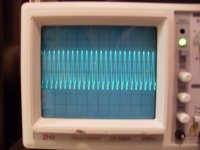
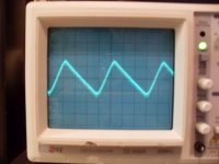
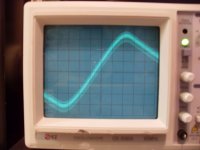
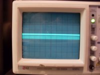
i've taken a few measurements of the amp, to clarify the issues i'm having.
a.) the scope is set to 1us/div and .1v/div here, showing the oscillation on the output (after the mosfet buffer, 20R load) with the inputs grounded.
b.) ripple voltage at the end of the unregulated supply showing a ~1vpp ripple at 120hz. you can clearly see the high-frequency oscillation riding on top of the ripple waveform.
c.) a closer view of the ripple with added hf oscillation.
d.) finally, the voltage at the output of the regulator V+ rail, showing 15.7vdc with essentially no noise other than the hf oscillation.
it seems i basically invited murphy into my home by paying little attention to layout and grounding in a design using a high-bandwidth, high slew rate opamp.
so i have a few ideas:
1.) swap the ad843 for an ad797, which has significantly better noise performance in the audio band and slightly better THD figures. the lower slew rate and bandwidth of the '797 would ease design requirements. does anyone have any opinions about differences in audio quality between these two chips?
2.) add a low-pass filter and high-pass filter to the inputs of the opamps to reduce the possibility of incoming signals pushing DC to the headphones or inducing hf oscillation. is this really necessary, considering the phase-lead capacitor in the feedback network?
3.) redesign the layout with a ground plane or star ground. it's easy to see that the circuit would greatly benefit from better grounding and layout, so i plan on experimenting first with this aspect of the circuit. soon, i'll finally have a nice dual-rail lab bench power supply to test bits and pieces of the design. i'll continue to post layouts with questions as i go.
~ brad.
Attachments
hi andrew, thanks for the comments.
decreasing the phase lead capacitor extends the bandwidth of the amplifier even more, right? the only reason i can understand doing that is in the context of also doing proposal 2.)... have i missed something?
also, caps that small are probably ceramic. is a C0G-type ceramic suited for duty inside the signal path?
thanks. a new one-channel-only-no-psu pcb layout is in the works to that end.
~ brad.
phase lead cap in the NFB loop. Try reducing it, in stages, to about 1/16 of present value.
decreasing the phase lead capacitor extends the bandwidth of the amplifier even more, right? the only reason i can understand doing that is in the context of also doing proposal 2.)... have i missed something?
also, caps that small are probably ceramic. is a C0G-type ceramic suited for duty inside the signal path?
Do all three proposals 1.) to 3.)
thanks. a new one-channel-only-no-psu pcb layout is in the works to that end.
~ brad.
This a very interesting thread and I just found it.
A few years ago I started experimenting with such circuits and I had designed them for High Voltages for esl's and es headphone use by stacking the fet's.
And I had just recently figured out how to build a fet ccs to replace the load resistor aswell as stacking the fet's in the ccs for HV use.
Excelent! Keep up the good work guy's. jer
i'm glad there's interest in the thread.
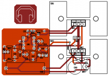
well, here's my first try at the layout for an isolated amp section. i went with a ground plane. it's my first attempt at such a thing, so let me know if there are any glaring mistakes.
thanks,
~ brad.
well, here's my first try at the layout for an isolated amp section. i went with a ground plane. it's my first attempt at such a thing, so let me know if there are any glaring mistakes.
thanks,
~ brad.
Attachments
interesting...
after playing around with the amp in a number of ways, i found that the hum left when an 8 ohm speaker load was connected instead of the 32 ohm headphones. i know i'm exposing my ignorance, but what could cause this?
with the 8 ohm load, the sound is very detailed and sharp. the bass is more impactful and controlled than you'd expect with such a low-impedance load. with that in mind, i simulated the THD for 0.5W into 8 ohms to be 0.0018%. not bad.
just thought it was interesting. makes me anxious to get the design working with headphones. this thing should sound really good.
~ brad.
after playing around with the amp in a number of ways, i found that the hum left when an 8 ohm speaker load was connected instead of the 32 ohm headphones. i know i'm exposing my ignorance, but what could cause this?
~ brad.
Grados are have much more sensitivity than any 8 ohm speaker
Grados are much more sensitive than any 8 ohm speaker
Ah, makes sense. Thanks.
I've built the single amp channel design and it measures well into a 20R dummy load, at least on what I can measure, using a lab bench power supply. No evidence of oscillation from DC to 30MHz. Frequency and phase response seem to adhere reasonably well to the design predictions. Noise at the scope's baseline and transient response is OK.
I'm more than happy to run extra tests if anyone has recommendations, but I am limited by my test equipment...
~ Brad.
Ah, makes sense. Thanks.
I'm more than happy to run extra tests if anyone has recommendations, but I am limited by my test equipment...
~ Brad.
I have a hard time measuring hum that shows up in Grados with my inexpensive equipment, so I'd say the one of the best tests for a headphone amp is to plug in a pair of grados set the volume a little louder than normal listening and run a silence track in a very quiet room.
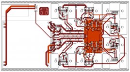
alright, it's been a while, i know. i'm a bit gun-shy after the previous revision.
nevertheless, here's the new board! i really need opinions on layout here. be as critical as you want; i'd rather have to fix the design now than after i spend more money on parts and wire it up...
i did my best to focus on grounding. notice the two 'star' points on the groundplane for earth, the capacitor bank, the regulated rails, and the headphone return. i connected the small-signal grounds straight to the groundplane. the +/-15V rails do follow semi-circuitous routes to their destinations, but i think it's OK.
also worth mention is that the board is designed for a hammond 1455-series enclosure, though which one escapes me at the moment.
~ brad.
nevertheless, here's the new board!
i really need opinions on layout here. be as critical as you want; i'd rather have to fix the design now than after i spend more money on parts and wire it up...i did my best to focus on grounding. notice the two 'star' points on the groundplane for earth, the capacitor bank, the regulated rails, and the headphone return. i connected the small-signal grounds straight to the groundplane. the +/-15V rails do follow semi-circuitous routes to their destinations, but i think it's OK.
also worth mention is that the board is designed for a hammond 1455-series enclosure, though which one escapes me at the moment.
~ brad.
Attachments
Last edited:
Has anyone tried to put the Szekerez inside an opamp FB loop ?
hahahaha!
 well you're in the right place.
you're quite right. the open-loop szekeres can be tweaked for ~0.1% THD, but bass response is poor due to input and output coupling capacitors, and phase shift is high in the khz range.
just go back a few posts to the last schematic i posted and you'll see an example of just what you propose. simulations show 0.0014% THD and flat phase/frequency response to ~50khz. (it sounds pretty good too, but i can't tell you specifics as i haven't listened using high-quality headphones and a good low-output impedance power supply.)
~ brad.
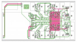
it's been a while...
alright, figured i should finally wrap this project up; i revisited the board layout and tweaked the power and ground traces, trying as much as possible to isolate high- and low-current ground returns. here's the revised board, in horrible neon...
i'll be ordering a pair of pcbs soon. build log and results to come shortly!
~ brad.
Attachments
- Status
- This old topic is closed. If you want to reopen this topic, contact a moderator using the "Report Post" button.
- Home
- Amplifiers
- Headphone Systems
- my take on the szekeres