@diegomj1973
Good points all. Thanks very much.
Re R2,R13,R15 : indeed - dunno what I was thinking there.
I got lazy on the bias network (R7.R8) just because... well, until figured I'd tidy it up later when it became a problem. Right now the PSRR doesn't depend on the noise through R8. Bigger issues yet, with the current sources. I added the 5 V ties as you suggested and it made a massive difference ... which I didn't expect and which means I don't fully understand this yet and need to go back to the drawing board.
I figured 5 V would only really work well with low impedance, high sensitivity phones, so the gain is set on the low end. The gain can be increased, but the amp isn't going to be particularly good with 300 ohms home headphones like the HD-600 as there is very limited voltage.
This is the only part I didn't follow. Could you explain why BC327/337 are no good here?
I could not open those .asc files, since I use Multisim for simulations.
Anyway, I upload the schematic of how it should be under my judgment.
The BC337 and BC327 in place of Q3 and Q4 can be used. In these places, the current and power requirements are very low (then , these transistors would not be very necessary ). The BC560C and BC550C have lower noise figure and better frequency response than BC337 and BC327.
R7 can be as low as 3,3 K. Then, R8 can be as low as 10 K.
regards
Attachments
Last edited:
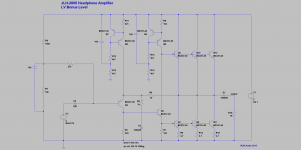
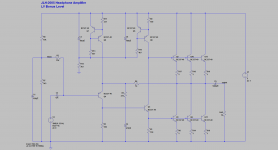
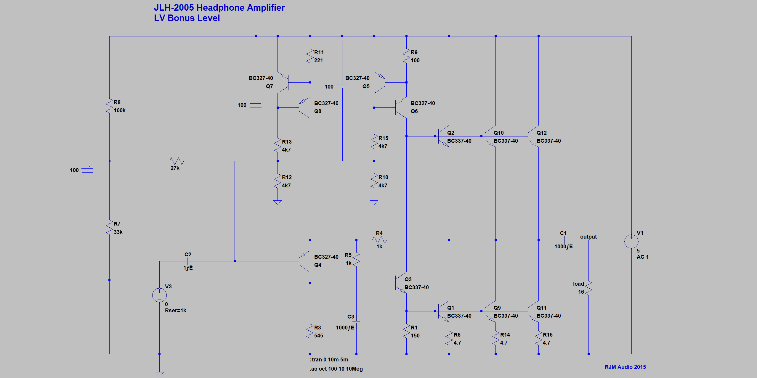
Good, everyone seems to be in broad agreement. I've mixed and matched the suggestions in the attached schematic. The values are hardly set in stone, I've just tried to use standard values where possible. (R3 is the only "tricky" one, it has to match the current source, so either it or the source current should be trimmable.)
I mean it's not going to win any contests, but I think it's a neat demo of how far you can get on 5 V.
Thanks again to everyone who helped out.
I mean it's not going to win any contests, but I think it's a neat demo of how far you can get on 5 V.
Thanks again to everyone who helped out.
Attachments
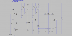
Good, everyone seems to be in broad agreement. I've mixed and matched the suggestions in the attached schematic. The values are hardly set in stone, I've just tried to use standard values where possible. (R3 is the only "tricky" one, it has to match the current source, so either it or the source current should be trimmable.)
I mean it's not going to win any contests, but I think it's a neat demo of how far you can get on 5 V.
Thanks again to everyone who helped out.
To have proper even harmonic cancellation in the quasi push-pull output stage after the phase splitter, the output devices top and bottom should be identical.
To be precise, if one include 1R degeneration on the bottom, one should do the same on top.
Especially with BJTs in parallel, the degeneration resistors is desirable, if not essential, to help current balancing.
IMHO there is no advantage to use 2 separate 100µ/4.7k RC filters (C3, C6, R12, R10) for biasing the two CCS.
That will save you two components.
Patrick
Last edited:
Hi Patrick,
Roger that!
Though the extra two components won't break the bank exactly, in the interests of a compact layout...
Further thought - is there a need for a compensation capacitor in there, or does the funky current feedback going on here mean some other scheme is needed to insure stability?
Roger that!
Though the extra two components won't break the bank exactly, in the interests of a compact layout...
Further thought - is there a need for a compensation capacitor in there, or does the funky current feedback going on here mean some other scheme is needed to insure stability?
Attachments
Member
Joined 2009
Paid Member
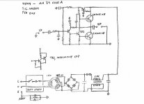
If you are interested in making it simpler then I'd suggest my TGM9 version SR. I've attached the schematic. The basic JLH works very well, I'm not convinced that the CCS are needed in a headphone amplifier. The first CCS has little impact on performane in my opinion, the 2nd helps with thermal stability - but for a low power version is this a concern ? The thing you do want is a good PSRR because sensitive headphones will pick up any rail noise and this is where my schematic helps - the emitter follower in the power rail greatly improves the PSRR for a quiet amplifier. Instead of beefy 2N3055's in the output, I would use a pair of nice TO-126 devices such as BD139. Some h.f. compensation (such as you have shown, or through the use of a Cdom at base-collector of TR3) will be needed.
Attachments
Last edited:
> The thing you do want is a good PSRR because sensitive headphones will pick up any rail noise
Precisely the reason for the Group of components around C1, C3 and C6, including the 2x CCS.
Other Advantage of the CCS's are described here :
http://sound-au.com/tcaas/jlhupdate.htm
Patrick
Precisely the reason for the Group of components around C1, C3 and C6, including the 2x CCS.
Other Advantage of the CCS's are described here :
http://sound-au.com/tcaas/jlhupdate.htm
Patrick
Last edited:
I could not open those .asc files, since I use Multisim for simulations.
Anyway, I upload the schematic of how it should be under my judgment.
The BC337 and BC327 in place of Q3 and Q4 can be used. In these places, the current and power requirements are very low (then , these transistors would not be very necessary ). The BC560C and BC550C have lower noise figure and better frequency response than BC337 and BC327.
R7 can be as low as 3,3 K. Then, R8 can be as low as 10 K.
regards
In scheme I uploaded, R13 and R12 should not be equal to R10 and R15. The first constant current source supplies less current than the second. R13 and R12 are optimized based on the expected change in current with the variation of the supply voltage and temperature . With R10 / R15 is the same story, but for other current value (R10 / R15 can take other values than those calculated for R13 / R12).
Then , it is not advisable to share bootstrap capacitors and resistors.
Even bootstrap capacitors may not be the same.
Regards
It can be simulated to verify what I 'm holding.
The effects of increasing resistance values of the bootstrap (up to a certain limit): the current increases with increasing supply voltage, at a lower rate. At the same time, the current decreases with increasing temperature, at a higher rate.
The effects of reducing the resistance of the bootstrap (up to a certain limit): the current increases with increasing supply voltage, at a higher rate. At the same time, the current decreases with increasing temperature, at a lower rate.
Regards
PD: resistance of the bootstrap = R12 + R13 or R10 + R15
Last edited:
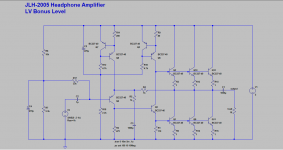
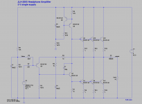
So here is my final attempt, since I consider the complementary circuit superior, whether at +/-15V or +5V only.
The circuit has quite some changes at both the input stage and the phase splitter, in order to lower even harmonics significantly.
The close loop response has way too much gain (overshoot) at 10MHz, even with a heavy 16R load.
So both bandwidth limiting in the feedback network, as well as output Zobel is added.
As it stands, it has clean frequency response even with no external load connected.
No such problems with the complementary version in #413.
Patrick
.
Attachments
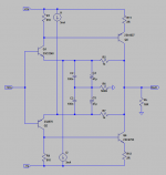
Well, if we are going there, then could we go here? (together with Patrick's low current operating points) added 220 pF compensation cap, removed front CCS, consolidated to (my) standard resistor values.
(As was noted #46 the first CCS doesn't seem to be needed.)
About 1 V rms and 60 mA available into 16 ohms. Nominal output power rating 60 mW. Much lower for high impedance phones of course.
(As was noted #46 the first CCS doesn't seem to be needed.)
About 1 V rms and 60 mA available into 16 ohms. Nominal output power rating 60 mW. Much lower for high impedance phones of course.
Attachments
Last edited:
You need to be careful though, too low a Q3 current and all hell may break loose when driving low-impedance loads, especially when beta droop kicks in at higher output currents. BC337 should easily be able to push 100 mA though, so 60 mA for 3 pairs does not sound critical.
For a low power amp like this, the assumption is that it is meant for in-ear phones.
I have not seen one that drop belows 16R in the audio band, for which the design is laid out.
So I do not see the point of much higher bias.
If anything, it will eat up voltage headroom, which I already not plentiful.
Only the NXP 337 has a flat hfe response, but 30mA is about the limit before it drops.
Fairchild does not even show a curve, and the On Semi looks like mountains.
Patrick
Last edited:
Hi I have just built this amp and so far it's sounding good, it's the blue PCB version 101101, can somebody tell me where the input caps on the board are please, possibly by marking it on a photo if possible? I would like to change it for something better.
Many thanks!
The input caps (1uF) are these:
An externally hosted image should be here but it was not working when we last tested it.
My kit included 470nF input caps. I have changed them for 1uF Panasonic metal film capacitors (1uF should be sufficient). Consider some of the modifications mentioned in this threat. Some will really augment the amplifier' sonical properties.
Last edited:
Thanks you so much that's great! Mine already has 470nF Poly caps there but may experiment with different caps like metal film as you suggested.
I'm still getting quite a bit of DC Offset at the outputs, should I put a couple of output caps in there? I read that 1000uf - 2200uf should be sufficient but do they need to be bi-polar? Do I just connect the positive output lead to one leg and the other leg to the centre terminal of the headphone jack?
Many thanks for your help.
I just noticed one of the smoothing caps was bulging so I decided to replace all 8 with 2200uf 25v Rubycon YXA capacitors but after re-assembling it would not power on!
I think they are low ESR caps after doing some research so maybe that's why it won't power on? I was told that low ESR caps pre/post regulators is a bad idea.
I think they are low ESR caps after doing some research so maybe that's why it won't power on? I was told that low ESR caps pre/post regulators is a bad idea.
- Home
- Amplifiers
- Headphone Systems
- JLH Headphone Amp