I've been working on and improving this circuit for the last 4 months or so. It's finally gotten to the point where it really feels "done", so I'm posting it.
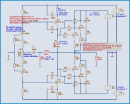
This is a very low distortion opamp suitable for driving relatively low-impedance loads. I use it for my 64-ohm ATH-A700s. It's a fully symmetric class-AB design using complementary BJTs. It's intended to run on +/-12v but could run on up to +/-20v. It uses garden variety TO-92 parts that are cheap and easily obtainable or substitutable - 2N3904/3906. It does use 40 transistors per channel, but they cost $0.04 each so it's not a big deal
Max recommended continuous output current draw is +/-100mA but it should be safe for momentary overloads up to 400mA or more. The output stage uses 4 paralleled sets of transistors, so it has good power dissipation. Iq in the output stage is 4mA/pair for a decently sized class-A region. Total quiescent current draw for the entire circuit is about 45mA. Everything runs cool at idle.
Topologically, this is a CFB opamp in disguise. It was originally based off of the LM6171, but has evolved from that design. A differential input voltage, buffered by a pair of diamond buffers, is converted to a differential error current which slews the compensation cap C1 at up to 100V/uS. A very linear darlington-input bootstrapped cascode diamond buffer (whew!) drives the load. With 86dB of OLG and an OL -3db of 4KHz (12MHz UGBW), lots of NFB can then be applied to bring the already very low distortion (-80db or better) from the output diamond buffer to incredibly low levels. Check out the closed-loop FFTs to see what I mean.
It is possible to shift the entire OLG curve around by changing the 4 resistors in the input stage (R1/R16/R17/R18). Lower them to 22 ohms for another 6db of gain at all frequencies. However, stability is best at 47 ohms; as shown, the prototypes have exactly 60 degrees of phase margin. Better layout should allow these values to come down more; Spice says that values of 10 or even 4.7 ohms should be possible.
I have had earlier versions of this circuit on an AP 2722, but have not had a chance to put this one on yet. It sounds extremely good; it has super clean treble and sibilance, which is where the last residual distortion components were in previous versions.
Zip file with schematic and FFTs:
http://www.ele.uri.edu/~simoneau/cfb1.zip
Attachments
homemodder said:Is this the topology that Lm6171 uses???
The frontend and gain stage are the same (although I use JFET CCSs), I added the degen resistors and redesigned the output stage completely.
Isn't this more or less an LT1363? It's like a classic current feedback amp with a diamond buffer in front of the feedback return/- input.
Have you tried it as both CFB and VFB? Was there any difference? I've thought about adding a diamond buffer to the -input of my le Classe A-like headphone amp just to find out if it sounds different as VFB.
Have you tried it as both CFB and VFB? Was there any difference? I've thought about adding a diamond buffer to the -input of my le Classe A-like headphone amp just to find out if it sounds different as VFB.
nelsonvandal said:Isn't this more or less an LT1363? It's like a classic current feedback amp with a diamond buffer in front of the feedback return/- input.
Yes, it is. However, my output stage is "fancier" (since most headphones do not require anywhere near rail-to-rail swing), and I have added degeneration all along the signal path. I also added the matching diodes/resistors on the (-) input diamond buffer - these should keep Vce on the input diamond buffers equal over the entire range of voltage swing. The matching network alone lowers the distortion by 6-10dB last I checked, and the output diamond buffer is some 30-50dB lower distortion than a simple 4-transistor version, depending on loading (!).
nelsonvandal said:
Have you tried it as both CFB and VFB? Was there any difference? I've thought about adding a diamond buffer to the -input of my le Classe A-like headphone amp just to find out if it sounds different as VFB.
I have never seriously tried it without the (-) diamond buffer. One major benefit that I see with the buffer is that any distortion in the input buffers will hopefully become CM and cancel out. Part of this depends on the JFETs being matched; my prototypes are matched for Idss=8mA +/-10%. It may be faster (and thus able to take more gain) without the buffer, but OL linearity will suffer.
homemodder said:Hi Sparcnut, 40 Trannies for a headphone amp
But I must say interesting topology you have as front end, very nice.
Had the same thought
40 transistors for low power amplifierI do not often use more than 6-15 T for these low power headphone/line amplifiers. 15 T would include my eventual transistors used for current sources, mirrors and voltage references = total number.
But if it works very well and adds some better performance: Why not? It is one personal choice of design.
-------------
I see there is some unique idea. I can not understand it right away.
I see one dual diamond differential input stage followed by one cascoded complementary output stage of parallelled TO-92.
This output is driven by two VAS stages. Q9 and Q11. They both cooperate in two different ways.
I say, that if it works it ashould render very high precision = low distortion. And if so, your design is well worth to try.
-----------------------
Just for compare:
I attach my own 200 mA class A output amplifier.
It has really great performance .. with fewer transistors.
Actually 10 Transistors + One RED LED
Lineup Transistor audio amplifiers
Attachments
lineup said:
Had the same thought
...
I say, that if it works it ashould render very high precision = low distortion. And if so, your design is well worth to try.
Well, it should have sub -150dbV distortion for 1Vrms into 50 ohms unity gain, and sub -170dbV for 0.1Vrms (normal volume on the A700s). Check the FFTs in the zip file. Both are well below the noise floor, which is about -100dbV in the audio band; -140dbV in 1hz bands.
I quickly simulated your design and got -90dbV distortion for 1Vrms into 50 ohms at +20db gain with dominant H2, is this about what you get?
This circuit certainly does work, the prototypes are 4 months old and have many (very pleasurable
) hours on them. I will post the AP results when I am able to run some tests. Previous versions agreed well with the Spice results, so I have high hopes for it.I should include some construction notes: It is very sensitive to power supply impedance at high frequencies. There are 3 diagonal crossings in the schematic, where the diamond buffer input transistors connect to the rails. I had to put 100pF silver micas directly across the rails (!), physically at the transistor leads, before it would stop oscillating. It became quite stable after doing that. Slewing has no odd effects other than the overshoot and ringing you would expect, given 60 degrees of phase margin.
Another strange problem I had was that one channel slewed in the positive direction much faster than the other. The "good" channel had symmetric +/-100V/uS slew rates; the "bad" channel was more like +25/-100. Replacing Q39 cured it. I must have managed to pull a bad transistor out of the bin...
- Status
- This old topic is closed. If you want to reopen this topic, contact a moderator using the "Report Post" button.
- Home
- Amplifiers
- Headphone Systems
- hybrid vfb-cfb headphone amp/driver