My building...still in development...
Hi friends,
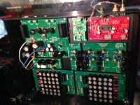
I am in the finishing stages of my Red Baron plus Tube-I-Zator with all the Salas power supply regulators. For me is a big task due to the parts count. I thouhgt that I could fix everything in one big case but it was impossible. I have to install the power transformers (3 in total ) in another case and run cables from there.
I am going today to setup the wiring and in the next few days I will finish the transformers case. Also I have to find a suitable and reliable way to connect both without electrical risks and also it have to be detachable. I am confident that it will sound very good....
Here is a (bad) iPhone photo...sorry...
Regards,
Jorge
Hi friends,
I am in the finishing stages of my Red Baron plus Tube-I-Zator with all the Salas power supply regulators. For me is a big task due to the parts count. I thouhgt that I could fix everything in one big case but it was impossible. I have to install the power transformers (3 in total ) in another case and run cables from there.
I am going today to setup the wiring and in the next few days I will finish the transformers case. Also I have to find a suitable and reliable way to connect both without electrical risks and also it have to be detachable. I am confident that it will sound very good....
Here is a (bad) iPhone photo...sorry...
Regards,
Jorge
Attachments
Not sure I am understanding your question, but I use a WaveIO card as the 'external' USB>I2S converter. Works very well with TDA1541A. Swapping is as easy as disconnecting the I2S cables and putting in a different source of I2S signal.
Yes. I don't want to built the usb transport in the case. Just interface the i2s thru a cable from outside the case.
Cases...
Hi,
I am using cases from Modushop in italy. If you make the holes and all that, are reasonably priced although the s/h can make it higher. It depends on what you whant and need. I am waiting from them a new case for a Hot Rod DCB1 preamp+ Vcpre from Rudi and I ordered with everything machined from them, more or less 160€ plus the taxes when the item arrives. Expensive, but I wanted that this preamp had the best pro looking because it is going to stay with me very long. The cases that sells the DiyAudio Store are from them...
Machining iron and aluminium is a very hard task, also you need a custom place to do it because it is very dirty and any kind of error, you pay it hard!!! So I went the easy route.
Regards,
Jorge
Great photo. Please take one of the other unit.
What case(s) are you using.
Hi,
I am using cases from Modushop in italy. If you make the holes and all that, are reasonably priced although the s/h can make it higher. It depends on what you whant and need. I am waiting from them a new case for a Hot Rod DCB1 preamp+ Vcpre from Rudi and I ordered with everything machined from them, more or less 160€ plus the taxes when the item arrives. Expensive, but I wanted that this preamp had the best pro looking because it is going to stay with me very long. The cases that sells the DiyAudio Store are from them...
Machining iron and aluminium is a very hard task, also you need a custom place to do it because it is very dirty and any kind of error, you pay it hard!!! So I went the easy route.
Regards,
Jorge
Yes. I don't want to built the usb transport in the case. Just interface the i2s thru a cable from outside the case.
According to John B. it is important to connect the DAC and the transport with the shortest possible traces, probably is not optimal having the i2s output far from de DAC.
Hi,
I am using cases from Modushop in italy. If you make the holes and all that, are reasonably priced although the s/h can make it higher. It depends on what you whant and need. I am waiting from them a new case for a Hot Rod DCB1 preamp+ Vcpre from Rudi and I ordered with everything machined from them, more or less 160€ plus the taxes when the item arrives. Expensive, but I wanted that this preamp had the best pro looking because it is going to stay with me very long. The cases that sells the DiyAudio Store are from them...
Machining iron and aluminium is a very hard task, also you need a custom place to do it because it is very dirty and any kind of error, you pay it hard!!! So I went the easy route.
Regards,
Jorge
Great, how about the size of the case(s) your using.
Case size...
Hi,
The DAC: Pessante 2U with 10mm front panel
Width: Structure 435 mm internal 430 mm
Depth: 300 mm Height: 80 mm
Weight: 4,3 KG
The Transformer Case:
Width: body 230mm, inner useful 210mm
Height: 80mm
Depth: 280mm
Weight: 2,0 KG
Regards,
Jorge
Great, how about the size of the case(s) your using.
Hi,
The DAC: Pessante 2U with 10mm front panel
Width: Structure 435 mm internal 430 mm
Depth: 300 mm Height: 80 mm
Weight: 4,3 KG
The Transformer Case:
Width: body 230mm, inner useful 210mm
Height: 80mm
Depth: 280mm
Weight: 2,0 KG
Regards,
Jorge
Hi friends,
I am in the finishing stages of my Red Baron plus Tube-I-Zator ..
Jorge
Beautiful!! It really fit nicely in that space. You will enjoy it for years!
Yesterday I fired it up finally for the 1st time ")
Wow... I even got some music at the output
Bad point is that there is so much noise/ hiss/ digital distortion (?!) and it's very loud!
Checked all the power supply, the voltages are correct.
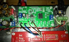
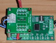
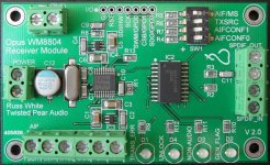
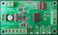
The settings on spdif transceiver are soldered as on the pics 2,3,4 (tried setting AIF/CONF0 to "-" but that didn't change anything, same noise).
I2S is connected in the following way:
BCK -> BCK
LRCK -> FS
DOUT -> Data
GND -> I2S GND
should be correct I suppose?!
Tried with a scope:
-square wave on spdif output of toslink converter
-BCK & LRCK showed square wave as well
-DOUT showed something weird (should it be square wave as well here?)
Would appreciate any advice!
Wow... I even got some music at the output
Bad point is that there is so much noise/ hiss/ digital distortion (?!) and it's very loud!
Checked all the power supply, the voltages are correct.
The settings on spdif transceiver are soldered as on the pics 2,3,4 (tried setting AIF/CONF0 to "-" but that didn't change anything, same noise).
I2S is connected in the following way:
BCK -> BCK
LRCK -> FS
DOUT -> Data
GND -> I2S GND
should be correct I suppose?!
Tried with a scope:
-square wave on spdif output of toslink converter
-BCK & LRCK showed square wave as well
-DOUT showed something weird (should it be square wave as well here?)
Would appreciate any advice!
Attachments
Newbe question - back to post 74!! DC restoration.
Hi Gents,
Sorry to butt in at this advanced juncture but i am not to "electronic" and a newbie to this hobby... but happily am in possession of one fully stuffed red baron DAC and one DC reference board (you know the small red one!!) and wish to use the DAC with the onboard I/V devices.- I have read through the thread and blog and think i understand what to do but just to be 100% certain! - adjusting the level for 0v on the DAC via its test points has been nicely explained (with a diagram) previously..however with regards to the connections of the small outboard DC restoring PCB:
1 . One wire from the DAC audio out (left or right-not "ref" center) can go to the center output (signal) of one phono sockets, the other side of the audio out to the + 5v input on the small PCB,... the other input to the small PCB is fed from the common GND (say from the DC Digital GND ).... hence 2 inputs to the Small PCB.
For the two outputs of the small PCB : + directly to the other phono output socket,..
The ref o/p to the common earth of both phono sockets...adjust both sides via each variable resistor for 0v such that no DC offset is seen between common Phone earth and any one of the two phono signal outputs (with no music playing!)
Er-- is that correct gents?
cheers for helping
Johnny
PS on my Red Baron PCB V 4.0 just above the" R" of the Red Baron legend is what seems to be two small lands ( A link) does this also have to be connected?
Hi Gents,
Sorry to butt in at this advanced juncture but i am not to "electronic" and a newbie to this hobby... but happily am in possession of one fully stuffed red baron DAC and one DC reference board
(you know the small red one!!) and wish to use the DAC with the onboard I/V devices.- I have read through the thread and blog and think i understand what to do but just to be 100% certain! - adjusting the level for 0v on the DAC via its test points has been nicely explained (with a diagram) previously..however with regards to the connections of the small outboard DC restoring PCB:1 . One wire from the DAC audio out (left or right-not "ref" center) can go to the center output (signal) of one phono sockets, the other side of the audio out to the + 5v input on the small PCB,... the other input to the small PCB is fed from the common GND (say from the DC Digital GND ).... hence 2 inputs to the Small PCB.
For the two outputs of the small PCB : + directly to the other phono output socket,..
The ref o/p to the common earth of both phono sockets...adjust both sides via each variable resistor for 0v such that no DC offset is seen between common Phone earth and any one of the two phono signal outputs (with no music playing!)
Er-- is that correct gents?
cheers for helping
Johnny
PS on my Red Baron PCB V 4.0 just above the" R" of the Red Baron legend is what seems to be two small lands ( A link) does this also have to be connected?
Yesterday I fired it up finally for the 1st time
Wow... I even got some music at the output
Bad point is that there is so much noise/ hiss/ digital distortion (?!) and it's very loud!
Checked all the power supply, the voltages are correct.
The settings on spdif transceiver are soldered as on the pics 2,3,4 (tried setting AIF/CONF0 to "-" but that didn't change anything, same noise).
I2S is connected in the following way:
BCK -> BCK
LRCK -> FS
DOUT -> Data
GND -> I2S GND
should be correct I suppose?!
Tried with a scope:
-square wave on spdif output of toslink converter
-BCK & LRCK showed square wave as well
-DOUT showed something weird (should it be square wave as well here?)
Would appreciate any advice!
I suppose that you have the 3.3v line conected where the old reclock circuit was, I mean, 3.3v to the digital DC input, ¿Is that right? Normally that noise issue is related to the BCK, make sure that the DAC chip receives it properly, and if that is the case check also FS, I do not mean the signal shape itself, I mean if the chip receives those signals properly, because it can happen that they are more attenuated than they should. If you feed digital DC input with 3.3v I think that you do not need that High Speed Buffer PCB, but I am not sure, better ask that to Oliver to be sure (If I am right and the board is not needed probably this is the source of your problem).
I see that you have implemented latest John suggested changes, you must use 1uF decoupling caps for the DEM system in order to work well (I tell you this because I think that you are using 1uF on the MSB and 220nF on the rest of the caps), otherwise you will have high levels of distortion, I do not think that is the source of your noise problem though, but 2.2nF free running oscillator cap must be used with 1uF decoupling caps.
Last edited:
Wargreymon
so it's 3.3v i2s attenuator mod as here. Everything is done as described by Oliver. The HSB in this case is not required.
could you please elaborate a bit how to check that?
Need to mention that the DEM mod hasn't been done yet.
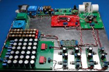
The layout is done to fit 4cm slim line from modu and to have some space left for Ian's boards:
so it's 3.3v i2s attenuator mod as here. Everything is done as described by Oliver. The HSB in this case is not required.
... I mean if the chip receives those signals properly...
could you please elaborate a bit how to check that?
Need to mention that the DEM mod hasn't been done yet.
The layout is done to fit 4cm slim line from modu and to have some space left for Ian's boards:
Attachments
Wargreymon
so it's 3.3v i2s attenuator mod as here. Everything is done as described by Oliver. The HSB in this case is not required.
could you please elaborate a bit how to check that?
Need to mention that the DEM mod hasn't been done yet.
The layout is done to fit 4cm slim line from modu and to have some space left for Ian's boards:
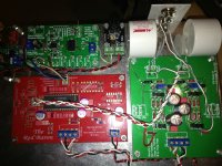
OK, as I have seen a image of the HSB on your previous post I thought that you had it installed, I now see that is just the image posted by Oliver some time ago.
By checking the signals on the chip I just mean that when you use the oscilloscope you put the probe directly on the pin/pins of the TDA1541A (In case you are not doing it like that of course), because the problem you describe can be a fault of the i2s attenuators, and if you check the signals directly on the PCB conectors where you connect the SPDIF module maybe you are seeing signals that are OK, but they get lost somewhere in the attenuators without reaching de TDA1541A, I happen to suffer the same problem yo have and it was mostly related with BCK not reaching the chip properly, I do not use TP SPDIF module though, I am using Teralink X2 until I decide on an asyncronus USB interface.
If you have not done the DEM clock mod then my previous post does not mean anything, I would recomend you using that last change though because at least in my case it made a tremendous difference in sound quality.
EDIT: Now that I see your latest images there are some diodes missing on the two diodes of the right (I am speaking about the i2s attenuators), you have a single diode installed in both positions where 3 diodes in series should be, unless there is something different when using TP SPDIF module... ¿You also have the 72HC02 installed? You must take it out.

Last edited:
Thanks! Will chech the tda chip then.
There are 3 diodes in series as should be, the picture shows only the top view with two diodes, the rest four pcs are below. Are you sure about the 72HC02 chip, the pic on Oliver's blog doesn't specify any info to remove it?!
OK about the diodes, as I can not see the bottom part did not think that where installed there.
About the 74HC02 I do not have it installed and my DAC works
 . Taking into account that you have removed all the circuitry associated with the DEM reclock circuit, I do not think it makes much sense to have that chip installed with the rest of the circuit out.
 Here you have the post of ECDesigns where it says that, I understand that "CMOS crap" is the 74HC02: http://www.diyaudio.com/forums/digital-line-level/79452-building-ultimate-nos-dac-using-tda1541a-477.html#post3411085
thanks, Wargreymon!
Will remove then today and check TDA chip as well.
thanks! The caps are the top point of the dac and are 4cm tall. The base is 3mm aluminum plate which is 400x320mm, so should fit the slim line. However I'm not sure about fitting Ian's FIFO, dual clock and the rest of the boards here. Anyway I would prefer to test the dac firstly as in original configuration and if it would be that good as everybody confirms, I'll contemplate about a taller case
Will remove then today and check TDA chip as well.
Nicely laid out. Will all that fit in one case?
thanks! The caps are the top point of the dac and are 4cm tall. The base is 3mm aluminum plate which is 400x320mm, so should fit the slim line. However I'm not sure about fitting Ian's FIFO, dual clock and the rest of the boards here. Anyway I would prefer to test the dac firstly as in original configuration and if it would be that good as everybody confirms, I'll contemplate about a taller case
Hi does anybody know if I have to re-arrange the 2sk216 pins before i solder them or just solder straight in on Red Baron v5?
You could solder the 2SK216 straight in. The design failure is corrected!
- Status
- This old topic is closed. If you want to reopen this topic, contact a moderator using the "Report Post" button.
- Home
- Group Buys
- "Reference" TDA1541A DAC with I2S-BUS architecture