Just reading this thread as I currently have fascination with CCSs. I've used Gary Pimm's CCS and find it such a versatile circuit and reportedly great sounding. How does this circuit equate with GP's circuit on the sonics?
I noticed your source for 2SK170BL was given as Donberg and as I'm in Ireland & I had a look & saw a pack of 5 2SK170BL for €6.99 and a pack of 5 2SK369 for €4.99 but no BL variant. I notice the 2SK170V variant is the higher IDSS category of 10-20mA and these are €4.99 for 5.
If the international shipping is high I can act as a shipping house for a group order if interested - just need to order some extra to cover my postage costs to wherever you are. Others have done this for me from the US so I'm happy (and surprised) to be able to return the favour
This project is stop for now because I'm in the process of selling my house. However, the interest seems to be so great, that I may start a group buy and have commercially made PCB.
I would also try to include the 2SK369-V FET that are difficult to source, maybe JKeny can help with that.
Don't forget that I still need to test the PCB design first")
I'm planning to test it this week.
I'll let you know.
Thanks...
I would also try to include the 2SK369-V FET that are difficult to source, maybe JKeny can help with that.
Don't forget that I still need to test the PCB design first
I'm planning to test it this week.
I'll let you know.
Thanks...
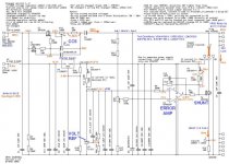
i am trying to digest the circuit. i am not up on all my ss circuitry. can someone tell me if my assumptions are correct.
t1/t2 and local circuitry is a ccs, t4 is the shunt element, u1 is the error amp. i am assuming that u4 is for regulating the 10.3v output and that t3 and t5 are for setting the voltages for u1.
i am not sure why one wants a 10.3v output. 12.6v i'd understand.
why use somewhat expensive/scarce jfets for t3 and t5, hasn't there got to be something cheaper and easier to source.
Yes, the PCB was corrected. In fact I tested the circuit last evening and it is working perfectly. So, the PCB is verified and ready to go.
There is so much interest in this board that I'll make a group buy and have a commercial PCB made. I'll produce the gerber and drill files tonight and send them for a quote tomorrow. Then I'll start a Group buy and we will see from there.
I'll also post a schematic with voltages readings soon. I tested the board with Vraw=250V, Vreg=235V, Rload=10K.
The way the actual board is configured (because of R3-R17 values), the minimum Vraw is 250V.
ackcheng said:There was a mistake with the original PCB posted on Emiles page. Is this version corrected for it?
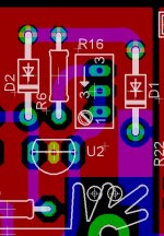
The mistake Arthur is referring to (I assume) is not the one described in the manual. In the PCB layouts originally posted on Emile's site, the anode of the TL431 (U2) needs to be disconnected from the end of the trace and then reconnected to the junction of R6 and D1. I can't tell immediately whether this has been corrected in Algar-emi's PCB, though on first glance the underside of the PCB in this area looks the same as in Emile's.
This error will affect the setting of the constant current, and not the output voltage, so may not be immediately apparent.
Alex
It is correct on my PCB, see image. Anode of U2 (TO-92 center pin) is connected to junction of R6-D1 (by the top (red) ground plane of the CSS section. This GND plane is the junction of R6 and D1 ,U2, D8 anodes. Thanks AlexM for the info.
Since I really didn't have the real PCB, I reproduced it using the schematic, and the general layout that I could figure out from the board user manual. So, I was able to reproduce the pcb errors as well
Take note that I rename D8 to D2 on my PCB and parts list.
I sent the PCB files today to get an estimate.
Attachments
- Home
- Group Buys
- HV Shunt Regulator PCB