Hi all,
This is a part of an exercise I try to solve,
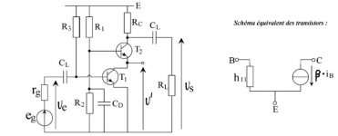
I have to draw the "equivalent small signal schematic" for this amp, and calculate the voltage gain from this small signal schematic
I'm totally lost. For a single transistor it's ok, but for a cascode I can't find how to calculate the gain
This is a part of an exercise I try to solve,
I have to draw the "equivalent small signal schematic" for this amp, and calculate the voltage gain from this small signal schematic
I'm totally lost. For a single transistor it's ok, but for a cascode I can't find how to calculate the gain
Attachments
Well as a pointer :
The purpose of a cascode transistor T2 is to prevent the voltage
swing at T1's collector that would normally occur, thus preventing
the miller effect reducing the bandwith of T1.
T2's base is clamped by the voltage source and the voltage swing
appears on T2's collector. As the voltage source should have very
low impedance the miller effect is less consequential here.
As T2's base is clamped so is its emitter effectively.
I gave up on equivalent circuits, finding them more confusing
than helpful beyond a certain point but they are important.
As stated the gain is near enough identical to a single transistor stage.
sreten.
The purpose of a cascode transistor T2 is to prevent the voltage
swing at T1's collector that would normally occur, thus preventing
the miller effect reducing the bandwith of T1.
T2's base is clamped by the voltage source and the voltage swing
appears on T2's collector. As the voltage source should have very
low impedance the miller effect is less consequential here.
As T2's base is clamped so is its emitter effectively.
I gave up on equivalent circuits, finding them more confusing
than helpful beyond a certain point but they are important.
As stated the gain is near enough identical to a single transistor stage.
sreten.The purpose of a cascode transistor T2 is to prevent the voltage
swing at T1's collector that would normally occur, thus preventing
the miller effect reducing the bandwith of T1.
agreed
T2's base is clamped by the voltage source and the votage swing
appears on T2's collector. As the voltage source should have very
low impedance the miller effect is less consequential here.
As T2's base is clamped so is its emitter effectively.
What voltage source? Remember, my answears have to be based on the equivalent circuit.
Bricolo said:[B
What voltage source? Remember, my answears have to be based on the equivalent circuit. [/B]
R1, R2 and Cd, at AC this is a low impedance voltage
source, a divided [R2/(R1+R2)] version of rail voltage E.
sreten.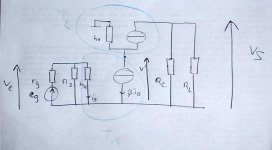
T2 divides T1's current by the ratio of its Beta.
So ib2 + B2.ib2 = B1.ib1
ib2(B2+1) = B1.ib1.
ib2 = B1.ib1/(B2+1)
B2.ib2= B2.B1.ib1/(B2+1)
Output current is very near a single transistor for high Beta.
Note also this is one of those very poor circuits only found
theory textbooks, as voltage gain is dependent on B1, this
sort of thing should only be used inside a feedback loop.
DC output voltage is also very poorly defined.
sreten.
So ib2 + B2.ib2 = B1.ib1
ib2(B2+1) = B1.ib1.
ib2 = B1.ib1/(B2+1)
B2.ib2= B2.B1.ib1/(B2+1)
Output current is very near a single transistor for high Beta.
Note also this is one of those very poor circuits only found
theory textbooks, as voltage gain is dependent on B1, this
sort of thing should only be used inside a feedback loop.
DC output voltage is also very poorly defined.
sreten.Thank you, that makes sense.
So, for a high beta (180 in this case) ic is nearly the same as with a single transistor
ib1 is also very close to ib2, so V' is equal to Ve am I right?
So T1 isn't really running at constant Vce, but if the voltage gain is important, the Vbe variations can be considered null.
BTW, what would be a better circuit, with no (or lower) beta dependance, and DC stability? (one that wouldn't require feedback)
BTW, what would be a better circuit, with no (or lower) beta dependance, and DC stability? (one that wouldn't require feedback)
Simply add an emitter resistor to T1. And use a proper voltage divider for its base.
Regards
Charles
phase_accurate said:
Simply add an emitter resistor to T1. And use a proper voltage divider for its base.
Regards
Charles
the need for a voltage divides on the base is obvious, but why the emirrer resistor?
I see one advantage in this: increasing the input impedance. Are there any other ones?
phase_accurate said:
Simply add an emitter resistor to T1. And use a proper voltage divider for its base.
Regards
Charles
And an emitter follower to the output, as gain is too
dependent on RL. For Audio cascoding T1 is fairly pointless.
But two transistor circuits work much better with feedback :
http://www.dself.dsl.pipex.com/ampins/discrete/twoq.htm
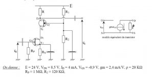
sreten.Another problem 
I have to calculate R and Rs.
Both transistors have the same bias points
Method1:
Vgs=-0.9V
Since Vg=0V, S is at 0.9V (23.1 for the upper transistor)
Id=4mA so R=Rs=U/I=0.9/0.004=225R
Right?
Method2:
Vds=8.5V
Id=4mA
So
E=R*Id+Vds+Vds+Rs*Id
-> 7V left for the resistors. 3.5V on each since the bias is identical for both transistors.
That gives Rs=R=3.5/0.004=875R
The results aren't the same for both methods
Attachments
- Status
- This old topic is closed. If you want to reopen this topic, contact a moderator using the "Report Post" button.
- Home
- General Interest
- Everything Else
- I've got difficulties to solve this electronic exercise