They often use resistors at the output for current limiting and there's normally at least one somewhere to set the idling currents, so why no input stage degeneration?
In fact chip designers seem to go out of their way to avoid using resistors as far as possible. Any thoughts?
In fact chip designers seem to go out of their way to avoid using resistors as far as possible. Any thoughts?
How do you know they don't? The schematic on the data sheet is just conceptual.
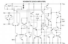
Well, here's the NE5532 schematic. No degeneration in the input pair, but plenty of other resistors shown. I don't claim to understand this schematic very well.
Attachments
Last edited:
Is it noise specification that over-rules all other design choices?
Do degeneration resistors actually add that much noise, if any at all? I don't know really. It doesn't seem to me that they'd add much if any noise.
1. Noise - especially an issue where the opamp is used in a high gain configuration
2. Maximize loop gain at LF (remember the DC performance of opamps is a large part of their utility value)
3. They most often use Cdom MC, so provided output loads are not unduly capacitive, they tend to be stable, so no need to use input stage degen to reduce loop gain enough to put the output stage pole below the UGF (pole splitting effect of Cdom MC helps here as well)
Others already mentioned above as well.
Possibly, but it's hard to imagine that chip real estate is such a big issue. Perhaps there's some difficulty in creating decent quality or close tolerance resistors. I notice that specifications that rely on resistors tend to be quite badly defined (e.g. quiescent current or max output current).Resistors use a lot of silicon?
That does seem to be the approach sometimes taken, but I'm still wondering why.Better to use three or four matched BJTs than a resistor.
Thanks, SY - That's good to know.Close tolerance is hard but close matching is easy.
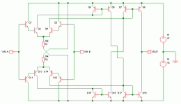
So for an opamp circuit like the one below, we don't know exactly what the idling currents of the two input stages are, but they will be closely matched (when the common mode input voltage is close to zero).
The main feature of the circuit is that the common mode input voltage range extends about 0.5V beyond the supply voltage in both directions.
The benefit of biasing the input stages with resistors is that as the common mode input voltage moves from rail to rail, control is handed over gradually from one input stage to the other, with the total transconductance remaining constant.
I'd been wondering how guilty to feel about the resistors, but it should be fine.
Attachments
- Status
- This old topic is closed. If you want to reopen this topic, contact a moderator using the "Report Post" button.
- Home
- General Interest
- Everything Else
- Why don't BJT IC opamps use resistive degeneration in the input stage?