So I really wonder if there's something I've entirely missed here ... How come they can make the output stage work up till 500 MHz when the coax cable's capacitance and inductance are considered ... ??
This really puzzles me so clarifying input from those of you who know is appreciated
Cheers,
Jesper
I suspect if you take the re of the last follower and the 43 Ohm resistor into account the output is match terminated or very close to it.
In this case it is exactly what I'm looking for, a 1 meg input, since the
crazy R&S doesn't have 50R input mode.
Internal terminators have an annoying tendency to get fried. External ones are much easier to replace.
Probably would require the LTC6268-10 chips and 100:1/100x
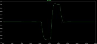
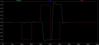
I've determined one thing after spending some time with Spice sims today. For this Linear Technology circuit it really does have to be the decompensated LTC6268-10 chips because the compensated LTC6268's can't keep up at 100MHz+, at least not with a 100MHz square wave. Probably would do better with a sine wave given the -3dB point at 350MHz.
In the first plot below all I have done is replace the LTC6268-10's in their circuit with their LTC6268 model. Pretty much the expected result. Damped and the rise time can't keep up (compare with the LTC6268-10 sim in post #1)
That means it really would have to be two 10x gain stages, along with the 100:1 input attenuator, since the -10's are gain of >10x stable. If I still want to use this circuit.") May be other better options!
May be other better options!
I did get the values worked out for a lower atten/gain version, the next two attachments. I decided on 100V max input instead of 500V, so a 20:1 attenuation with each stage gain set to sqrt(20) = 4.47x. I wanted to bump the input Z up a bit. I settled on a 76.8K/(4.99K || 17.4K) = 19.8:1 divider set. The gain set then turned out to be 17.4K and the 4.99K, (17.4K/4.99K +1) = 4.49x per stage, 4.49^2 = .20.2x total.
Biasing it took a bit of head scratching. After doing all sorts of algebra it turns out what LT did works in general. Just take the feedback resistor, 17.4K, double it to 34.8K, and use that as the divider that sets the stage 1 bias. Works great. The goal for stage 1 is a 2.5V output bias point of course, half the supply, so the input DC bias needs to be 2.5V/4.48 = 0.558V. Using the two 38.4K divider resistors with the bottom in parallel with the 4.99K does exactly that.
Same thing applies to the second stage bias, still shooting for 2.5V output bias point and 0.558V input bias. Leaving their 10K on the bottom of the divider that works out to be 80.6K for the top.
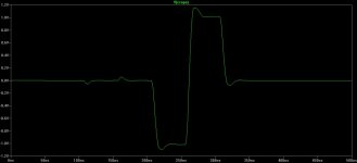
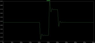
The resulting output works, sort-of. Has the same problem of not keeping up with the rise time. But the worse problem is the LT circuit seems **extremely** sensitive to tiny amounts of parasitic capacitance in various locations. For example, notice the 0.1pF I have across the two feedback resistors. The next plot shows what happens without those. Geezzz - 0.1pF, that is likely the capacitance of a 0805 resistor! So I'm not really sure the LT circuit is real-world viable. I never made it to trying input capacitors in parallel with the 76.8K's.
The final plot shows why there are two small wiggles before the square wave on the circuit output. The green is the output of the probe circuit, while the red and blue are the input voltage sources LT has set up. They have both doing a dip together between 100ns and 150ns, to show the differencing amp really will cancel them out. Almost does except for those wiggles. This is with the 0.1pF feedback capacitors added back, notice that without those the wiggles don't show up.
I've determined one thing after spending some time with Spice sims today. For this Linear Technology circuit it really does have to be the decompensated LTC6268-10 chips because the compensated LTC6268's can't keep up at 100MHz+, at least not with a 100MHz square wave. Probably would do better with a sine wave given the -3dB point at 350MHz.
In the first plot below all I have done is replace the LTC6268-10's in their circuit with their LTC6268 model. Pretty much the expected result. Damped and the rise time can't keep up (compare with the LTC6268-10 sim in post #1)
That means it really would have to be two 10x gain stages, along with the 100:1 input attenuator, since the -10's are gain of >10x stable. If I still want to use this circuit.
May be other better options!I did get the values worked out for a lower atten/gain version, the next two attachments. I decided on 100V max input instead of 500V, so a 20:1 attenuation with each stage gain set to sqrt(20) = 4.47x. I wanted to bump the input Z up a bit. I settled on a 76.8K/(4.99K || 17.4K) = 19.8:1 divider set. The gain set then turned out to be 17.4K and the 4.99K, (17.4K/4.99K +1) = 4.49x per stage, 4.49^2 = .20.2x total.
Biasing it took a bit of head scratching.
After doing all sorts of algebra it turns out what LT did works in general. Just take the feedback resistor, 17.4K, double it to 34.8K, and use that as the divider that sets the stage 1 bias. Works great. The goal for stage 1 is a 2.5V output bias point of course, half the supply, so the input DC bias needs to be 2.5V/4.48 = 0.558V. Using the two 38.4K divider resistors with the bottom in parallel with the 4.99K does exactly that.Same thing applies to the second stage bias, still shooting for 2.5V output bias point and 0.558V input bias. Leaving their 10K on the bottom of the divider that works out to be 80.6K for the top.
The resulting output works, sort-of. Has the same problem of not keeping up with the rise time. But the worse problem is the LT circuit seems **extremely** sensitive to tiny amounts of parasitic capacitance in various locations. For example, notice the 0.1pF I have across the two feedback resistors. The next plot shows what happens without those. Geezzz - 0.1pF, that is likely the capacitance of a 0805 resistor! So I'm not really sure the LT circuit is real-world viable. I never made it to trying input capacitors in parallel with the 76.8K's.
The final plot shows why there are two small wiggles before the square wave on the circuit output. The green is the output of the probe circuit, while the red and blue are the input voltage sources LT has set up. They have both doing a dip together between 100ns and 150ns, to show the differencing amp really will cancel them out. Almost does except for those wiggles. This is with the 0.1pF feedback capacitors added back, notice that without those the wiggles don't show up.
Attachments
Last edited:
Hi again,
Quoting my own question:
... I would like to thank Udo & Scott for following up on this - and additionally Udo for clarifying the P6202 probe's design specifics
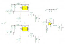
As it is I'm reasonably familiar with the concept of e.g. cable impedances, however, I didn't have a model for a coax cable that I could use to (reasonably) reliably simulate the load that the cable presents to the probe circuitry. But now - using my eyes - I noticed the cable circuitry used in agdr's #1 attachment - i assume it's reasonably realistic for a coax cable ...
Also, searching today for a probe circuitry I came across a link from calvin for a 1 GHz differential DIY probe:
https://xellers.wordpress.com/electronics/1ghz-active-differential-probe/
Schematic is attached to this post - and also can be found about 1/3 down the page.
I haven't read all of the design description but am thinking that it looks pretty neat ... Maybe interesting to progress with?
... One of you BTW know if a Rohde & Schwarz ZWOB 5 polyskop (100 kHz - 2.7 GHz) may be useful as an HF/RF oscilloscope? And if so - any shortcomings to using it in practice ... Asking because there's one available at a quite reasonable price close to where I live ...
Cheers,
Jesper
Quoting my own question:
So I really wonder if there's something I've entirely missed here ... How come they can make the output stage work up till 500 MHz when the coax cable's capacitance and inductance are considered ... ??
This really puzzles me so clarifying input from those of you who know is appreciated
... I would like to thank Udo & Scott for following up on this - and additionally Udo for clarifying the P6202 probe's design specifics
As it is I'm reasonably familiar with the concept of e.g. cable impedances, however, I didn't have a model for a coax cable that I could use to (reasonably) reliably simulate the load that the cable presents to the probe circuitry. But now - using my eyes
- I noticed the cable circuitry used in agdr's #1 attachment - i assume it's reasonably realistic for a coax cable ... Also, searching today for a probe circuitry I came across a link from calvin for a 1 GHz differential DIY probe:
https://xellers.wordpress.com/electronics/1ghz-active-differential-probe/
Schematic is attached to this post - and also can be found about 1/3 down the page.
I haven't read all of the design description but am thinking that it looks pretty neat ... Maybe interesting to progress with?
... One of you BTW know if a Rohde & Schwarz ZWOB 5 polyskop (100 kHz - 2.7 GHz) may be useful as an HF/RF oscilloscope? And if so - any shortcomings to using it in practice ... Asking because there's one available at a quite reasonable price close to where I live ...
Cheers,
Jesper
Attachments
https://xellers.wordpress.com/electronics/1ghz-active-differential-probe/[/URL]
Good find! His writeup applies to the Linear Tech circuit:
The first thing that becomes apparent when thinking about designing the differential amplifier is that a single opamp configured as a differential amplifier doesn’t make for a very good probe because there is a tradeoff between bandwidth and input impedance. The larger you make the gain-setting resistors, the higher the input impedance, but the feedback path is slowed down because the pole created by the feedback resistance and opamp input capacitance moves to the right when the feedback resistance is increased. To put that in more human terms, the feedback resistance and input capacitance form a lowpass filter, which slows down the opamp. Because we desire an extremely high input impedance, a single opamp is impractical. What can we do?
Yeah, this is why so many of these probe circuits are configured as instrumentation amps.
For your original problem of measuring oscillations, a small coil and a spectrum analyzer or a radio detector would be a good solution too.
Now there is a really good idea! That hadn't occurred to me. You are right, at these high oscillation frequencies they may radiate enough for pickup with a RF probe. Also solves the problem of no direct connections to the circuit, which in turn could stop or change the oscillation. Coupling to the RF probe could probably do the same, but I would suspect not to the degree of a direct probe connection. Hmm....
Last edited:
Internal terminators have an annoying tendency to get fried. External ones are much easier to replace.
I think you hit the nail on the head. The new R&S scope is targeted at the education market, from the marketing literature. The first thing the students would do in lab is measure a high voltage on the 50R setting and fry the terminator.
Only having the 1meg input is a lot safer.For RF pickup you don't want an RF probe (they are detectors for RF voltages) but a few turns of wire around 1/2" to 1" coupled directly to a BNC cable. In the past CB receivers were great for this and FM tuners on a dead channel also work well. Grid dip meters are also helpful in finding and fixing some oscillations (this is going way back).
Hi - & good morning all ...
@agdr:
Interesting - I didn't know that, actually ... However, as it happened I tried yesterday to configure the LTC6268 in an instrumentation set up and I think I got to some quite interesting results (attachments).
But before writing about this, I'd just like to add that I personally am interested in two different probes (agdr please see below):
1. One that is high bandwidth (500 MHz -> 1 GHz; gain ~ x1) and still does have minimum effect on the circuitry on which it is used ...
2. One that has a good deal of amplification while still having a very wide bandwidth. E.g. 50* amplification and >= 100 MHz bandwidth.
With respect to the first probe I notice that one of the challenges appears to be that the input impedance of most all probes I have looked at drops significantly when going up in frequency. Thus it may be around 250 ohms at 500 MHz - 1 GHz. This will influence the measurements I would like to make.
One way to overcome this may be to place a suitable value resistor in front of the input FETs - likely with a reduction in bandwidth due to FET input capacitance. So what to do if low circuitry influence and wide bandwidth is desired .... ?? Is there a FET/something else with very, very low input capacitance (fF region) that is suitable for this application?
I also notice udok's suggestions earlier ...
This could be interesting due to its simplicity and potentially very small size.
@udok: WRT the coax cable divider: How large a division is possible in practice while maintaining wide bandwidth (>= 500 MHz)? Could it be e.g. 5kohms? And won't it be noisy in practice?
And - if I decide to go with an already made single-ended probe (500 MHz to 1 GHz) ... may you then suggest a normally ebay-available probe that connects directly to a typical BNC oscilloscope connector? I can make a PSU if it's accessible to "get into" the probe ...
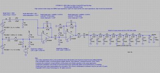
With respect to the second probe - the amplification probe ... I yesterday simulated the LTC6268 in an instrumentation amplifier setup - with some parasitics involved that I hope are reasonably realistic if a careful layout is made (pls. see schematic). Additional to the capacitances shown on the schematic I also tried inserting small inductances (1n - 4nH) in series with the resistors in the second section of the instrumentation amp - with no discernible effect.
However, what's interesting to me with this simulation is that even with 1p input capacitors in series with the 1k2 resistors it's got a - 3 dB point of ~ 120 MHz - and an amplification of 33.6 dBs (~48x). If the input capacitance is raised to 10 p the amplification is ~ x70 with no change in the simulation.
As can be seen from the pulse simulation it's still got some quite low level ringing - but considered that it is a 1ns pulse I think it is quite good (or?). And it has got a differential 2.4 k input impedance (at least) at 150 MHz ...
Any comments ... does this look feasible in practice or ... ? Any ideas for an input protection circuitry that will not degrade the performance?
WRT a ~gain x1 differential probe I also was able to simulate this up to ~ 500 MHz bandwidth - but with more wrinkles. I suppose though that it can/might be done with careful selection of component values ...
@agdr: I hope it's ok with you that I - to some extent - join in on your thread .. I realize I may have a slightly different aim than you have so if you prefer I start a separate thread let me know
Cheers,
Jesper
@agdr:
Yeah, this is why so many of these probe circuits are configured as instrumentation amps.
Interesting - I didn't know that, actually ... However, as it happened I tried yesterday to configure the LTC6268 in an instrumentation set up and I think I got to some quite interesting results (attachments).
But before writing about this, I'd just like to add that I personally am interested in two different probes (agdr please see below):
1. One that is high bandwidth (500 MHz -> 1 GHz; gain ~ x1) and still does have minimum effect on the circuitry on which it is used ...
2. One that has a good deal of amplification while still having a very wide bandwidth. E.g. 50* amplification and >= 100 MHz bandwidth.
With respect to the first probe I notice that one of the challenges appears to be that the input impedance of most all probes I have looked at drops significantly when going up in frequency. Thus it may be around 250 ohms at 500 MHz - 1 GHz. This will influence the measurements I would like to make.
One way to overcome this may be to place a suitable value resistor in front of the input FETs - likely with a reduction in bandwidth due to FET input capacitance. So what to do if low circuitry influence and wide bandwidth is desired .... ?? Is there a FET/something else with very, very low input capacitance (fF region) that is suitable for this application?
I also notice udok's suggestions earlier ...
- You can build a simple voltage divider probe: 500 Ohm R into 50 Ohm Coax cable => very high bandwidth
This could be interesting due to its simplicity and potentially very small size.
- You do not need a differential probe for this application,
active single ended < 1GHz is cheap on Ebay
@udok: WRT the coax cable divider: How large a division is possible in practice while maintaining wide bandwidth (>= 500 MHz)? Could it be e.g. 5kohms? And won't it be noisy in practice?
And - if I decide to go with an already made single-ended probe (500 MHz to 1 GHz) ... may you then suggest a normally ebay-available probe that connects directly to a typical BNC oscilloscope connector? I can make a PSU if it's accessible to "get into" the probe ...
With respect to the second probe - the amplification probe ... I yesterday simulated the LTC6268 in an instrumentation amplifier setup - with some parasitics involved that I hope are reasonably realistic if a careful layout is made (pls. see schematic). Additional to the capacitances shown on the schematic I also tried inserting small inductances (1n - 4nH) in series with the resistors in the second section of the instrumentation amp - with no discernible effect.
However, what's interesting to me with this simulation is that even with 1p input capacitors in series with the 1k2 resistors it's got a - 3 dB point of ~ 120 MHz - and an amplification of 33.6 dBs (~48x). If the input capacitance is raised to 10 p the amplification is ~ x70 with no change in the simulation.
As can be seen from the pulse simulation it's still got some quite low level ringing - but considered that it is a 1ns pulse I think it is quite good (or?). And it has got a differential 2.4 k input impedance (at least) at 150 MHz ...
Any comments ... does this look feasible in practice or ... ? Any ideas for an input protection circuitry that will not degrade the performance?
WRT a ~gain x1 differential probe I also was able to simulate this up to ~ 500 MHz bandwidth - but with more wrinkles. I suppose though that it can/might be done with careful selection of component values ...
@agdr: I hope it's ok with you that I - to some extent - join in on your thread .. I realize I may have a slightly different aim than you have so if you prefer I start a separate thread let me know
Cheers,
Jesper
Attachments
Last edited:
remember that you need a dc return on the + inputs
Thanks Gerhard - obviously should be there! 10 Mohm possibly?
and the 1pF coupling caps don't make much sense.
Ok - can I ask you what you otherwise think of the design?
Jesper
10 Meg are ok.
It's not too far away from the one from the data sheet of the ADA4817-1/ADA4817-2 that
I put on FR-4. I did not spend too much thought into it; all I really wanted was a buffer to
measure the Vgs of my IF3602 low noise amplifier without Heisenberging it.
The LT6082 seems to be a cmos op amp, its noise voltage is specc'ed at 4nV/rtHz at
1MHz. But the 1/f corner is not much lower, so, at 100 Hz you can expect a lot of noise.
Also, it is stable for gain > 10 only.
The output low pass seems to stand for the coax cable. Such a structure represents
a transmission line only for a large amount of sections, and it does not represent the losses.
A 50 Ohm resistor looked at through a lossless 50 Ohm cable looks like 50 Ohm,
so set your scope to 50R input, not 1 Meg. The op amp output with lots of feedback
is mostly 0, so use 50 Ohms at its output to terminate the source side properly.
The op amp then sees real 100 Ohm of load, and your scope sees only 50%
of the op amp output.
If your op amp is able to drive sth. like 100 Ohm, you should make the feedback
resistors smaller, esp. in the first stage. Less noise and less phase shift.
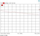
From the lossless CLCLCLCLCLC representation you would expect the loss of the cable
to be 0 until some very high frequency and then fall like rock. But that is not the way
losses in cables behave. I have just put 1 meter of a RG174-class cable on the
network analyzer. I do not know exactly what it is, bought it with SMA connectors
for some harmless interconnects. Teflon cable looks the same, it is no way better.
I did not bother to recalibrate the VNA.
You see a slow droop and this is hard to compensate for with RC filters since they
go 6 dB/decade up and down, or multiples thereof.
Bed time.
\gerhard
It's not too far away from the one from the data sheet of the ADA4817-1/ADA4817-2 that
I put on FR-4. I did not spend too much thought into it; all I really wanted was a buffer to
measure the Vgs of my IF3602 low noise amplifier without Heisenberging it.
The LT6082 seems to be a cmos op amp, its noise voltage is specc'ed at 4nV/rtHz at
1MHz. But the 1/f corner is not much lower, so, at 100 Hz you can expect a lot of noise.
Also, it is stable for gain > 10 only.
The output low pass seems to stand for the coax cable. Such a structure represents
a transmission line only for a large amount of sections, and it does not represent the losses.
A 50 Ohm resistor looked at through a lossless 50 Ohm cable looks like 50 Ohm,
so set your scope to 50R input, not 1 Meg. The op amp output with lots of feedback
is mostly 0, so use 50 Ohms at its output to terminate the source side properly.
The op amp then sees real 100 Ohm of load, and your scope sees only 50%
of the op amp output.
If your op amp is able to drive sth. like 100 Ohm, you should make the feedback
resistors smaller, esp. in the first stage. Less noise and less phase shift.
From the lossless CLCLCLCLCLC representation you would expect the loss of the cable
to be 0 until some very high frequency and then fall like rock. But that is not the way
losses in cables behave. I have just put 1 meter of a RG174-class cable on the
network analyzer. I do not know exactly what it is, bought it with SMA connectors
for some harmless interconnects. Teflon cable looks the same, it is no way better.
I did not bother to recalibrate the VNA.
You see a slow droop and this is hard to compensate for with RC filters since they
go 6 dB/decade up and down, or multiples thereof.
Bed time.
\gerhard
Attachments
Last edited:
All cables have something like that characteristic unless they have some special compensation in the design (e.g. Gore Eye-opener). The loss curve for CAT 3 through CAT 6 network cable is the same and pretty steep. Its just a more precise loss at HF with CAT 6.
Passive and active equalizers are a complex solution and not useful for this.
What is the real analog bandwidth of the target scope? Most probes are designed to that bandwidth and crash above it. Also not commonly known is that divider probes use resistance wire for the core as part of the HF extension. I'm not sure how that works. I think its explained in a training doc from Tek in the 1970's.
A P.S.: I know this is really basic but somehow it doesn't reply itself in my mind ...
How does a capacitor "scale" if it's connected via a resistor? E.g. how does a transmitting amplifier "see" a 10 nF capacitor connected via a 100 ohm resistor ... ? I would guess that it's the 10nF capacitor's impedance (at a given frequency) divided by the 100 ohms, i.e. it is "seen" as 100 pF. Isn't that correct?
Uh ... really basic but nevertheless just resurfaces in my mind ...
Cheers & thanks for maybe reading & replying ;-)
Jesper
Last edited:
Hi all,
I've been working a bit more on the notion of an HF probe - more specifically a 1 GHz HF probe and may/might have progressed some. However, the current work-in-progress probe is not a differential probe - it's single-ended but since it looks as if the thread is otherwise on pause (?) I take the liberty of posting more comments here as the thread start is relatively recent.
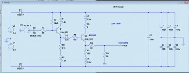
Since my last post I've been simulating a circuitry basically looking like the attached one. Please note that I have not attempted to DC stabilize it so DC offset is not stable ... The inductors are estimated trace inductances.
This circuitry is virtually linear from 1 kHz to appr. 1.5 GHz (- 3dB points), yet contrary to what appears to be common design practice it is based on two RF NPN transistors AND a quite high coupling capacitance compared with typical FET based probes. The high upper frequency cut-off is due to the very low input capacitance of the BUF660 transistor.
The advantage of this approach - as far as I can see & simulate - is that the current load on the DUT circuitry being measured is relatively constant over the full useable bandwidth. E.g. a 2 Vpp swing on the input loads the measured circuitry with appr. 120 uA p-p at 10 kHz and up to ~ 300 MHz. At 1 GHz the current load is ~230 uA p-p.
A FET probe (a generalization - but from what I can see in diagrams) appears to load the circuitry with e.g. 0.1uA p-p at 10 kHz but at 1 GHz the load may be more than 10 mA p-p. This appears to be less feasible to me as the very HF region is exactly where I'd like to measure and know what is going on without altering the DUT circuitry's response ...
And I'm thinking that loading the DUT circuitry with e.g 10 mAs at 1 GHz must change the way the circuitry responds to "being measured" - and possibly also change the distribution of frequencies present in the circuitry so that one actually measures "something different" from what would be the case if no FET probe was probing the DUT circuitry ...
In the attached probe circuitry the load on the DUT circuitry at lower frequencies is somewhat higher than if a FET probe is used - but where I reckon a digital circuitry is really noisy and emitting EMR when loaded - i.e. the HF/RF frequencies - the load is much lower (appr. 1/100). I admittedly am biased towards it
The "only" thing is "what" the 10 nF capacitor looks like from the DUT circuitry? Since - as I can see it - a main idea behind the use of a FET probe is the low capacitance load on the DUT circuitry - the circuitry I'm considering has a much higher capacitance - yet this is "moderated" by the series resistor.
To get an idea about this I've been looking into the basic capacitor formulas (q=C*v), and if v is substituted with R*i (q=C*(~6kohm)*i) it looks as if both q and i drops significantly - and thus the load on the DUT circuitry. While maintaining the lower cutoff frequency.
BUT since nobody else does it this way I realize I may be overlooking something here ...
Does it work or ... ?
Hope you will comment.
'Best for your weekend
Jesper
I've been working a bit more on the notion of an HF probe - more specifically a 1 GHz HF probe and may/might have progressed some. However, the current work-in-progress probe is not a differential probe - it's single-ended but since it looks as if the thread is otherwise on pause (?) I take the liberty of posting more comments here as the thread start is relatively recent.
Since my last post I've been simulating a circuitry basically looking like the attached one. Please note that I have not attempted to DC stabilize it so DC offset is not stable ... The inductors are estimated trace inductances.
This circuitry is virtually linear from 1 kHz to appr. 1.5 GHz (- 3dB points), yet contrary to what appears to be common design practice it is based on two RF NPN transistors AND a quite high coupling capacitance compared with typical FET based probes. The high upper frequency cut-off is due to the very low input capacitance of the BUF660 transistor.
The advantage of this approach - as far as I can see & simulate - is that the current load on the DUT circuitry being measured is relatively constant over the full useable bandwidth. E.g. a 2 Vpp swing on the input loads the measured circuitry with appr. 120 uA p-p at 10 kHz and up to ~ 300 MHz. At 1 GHz the current load is ~230 uA p-p.
A FET probe (a generalization - but from what I can see in diagrams) appears to load the circuitry with e.g. 0.1uA p-p at 10 kHz but at 1 GHz the load may be more than 10 mA p-p. This appears to be less feasible to me as the very HF region is exactly where I'd like to measure and know what is going on without altering the DUT circuitry's response ...
And I'm thinking that loading the DUT circuitry with e.g 10 mAs at 1 GHz must change the way the circuitry responds to "being measured" - and possibly also change the distribution of frequencies present in the circuitry so that one actually measures "something different" from what would be the case if no FET probe was probing the DUT circuitry ...
In the attached probe circuitry the load on the DUT circuitry at lower frequencies is somewhat higher than if a FET probe is used - but where I reckon a digital circuitry is really noisy and emitting EMR when loaded - i.e. the HF/RF frequencies - the load is much lower (appr. 1/100). I admittedly am biased towards it
The "only" thing is "what" the 10 nF capacitor looks like from the DUT circuitry? Since - as I can see it - a main idea behind the use of a FET probe is the low capacitance load on the DUT circuitry - the circuitry I'm considering has a much higher capacitance - yet this is "moderated" by the series resistor.
To get an idea about this I've been looking into the basic capacitor formulas (q=C*v), and if v is substituted with R*i (q=C*(~6kohm)*i) it looks as if both q and i drops significantly - and thus the load on the DUT circuitry. While maintaining the lower cutoff frequency.
BUT since nobody else does it this way I realize I may be overlooking something here ...
Does it work or ... ?
Hope you will comment.
'Best for your weekend
Jesper
Attachments
Last edited:
but since it looks as if the thread is otherwise on pause (?) I take the liberty of posting more comments here as the thread start is relatively recent.
The thread is definitely on pause. I've decided against that LT circuit I was looking at and I've moved onto other things. So please do feel free to post anything probe-related in general!
Last edited:
For what its worth
1) FETs are less sensitive to EMI
2) if you pick the right JFET for the input the input Z will be lowest. The HF issue comes from the input capacitance. At 1 GHz 1 pF = 159 Ohms. The real world is more complex than this. Even the dielectric changes at these frequencies.
What are you looking at?
1) FETs are less sensitive to EMI
2) if you pick the right JFET for the input the input Z will be lowest. The HF issue comes from the input capacitance. At 1 GHz 1 pF = 159 Ohms. The real world is more complex than this. Even the dielectric changes at these frequencies.
What are you looking at?
@agdr:
@1audio: Thanks for your feedback ...
Hmmm ... ok. But I'm actually looking to increase the Zin as I want my measurements to have the least possible effect on the circuitry I'm measuring. Thus also the resistor in the input ... But if you know of a JFET/"FET" with ~0.25 pF input capacitance that could be interesting (not sure it exists ...?)
To this end I was close to buying a Tektronix SCA-803 (network analyzer) last week but I didn't have enough time to familiarize myself with its functionality and so decided to let it go. But I am looking for a way to look at "various phenomena" with high speed and resolution (possibly could also be a spectrum analyzer - just don't know which one) - and, as you've probably noticed, also a reliable way to look at jitter also at the oscillator's output ...
Have a good day, both of you
Jesper
... Good to have it confirmed - thanks!The thread is definitely on pause. I've decided against that LT circuit I was looking at and I've moved onto other things. So please do feel free to post anything probe-related in general!
@1audio: Thanks for your feedback ...
2) if you pick the right JFET for the input the input Z will be lowest.
Hmmm ... ok. But I'm actually looking to increase the Zin as I want my measurements to have the least possible effect on the circuitry I'm measuring. Thus also the resistor in the input ... But if you know of a JFET/"FET" with ~0.25 pF input capacitance that could be interesting (not sure it exists ...?)
I'm hoping to learn. One thing is theory (to the extent that I'm familiar with, and understand, this) but I like to measure to verify that things are as assumed - and also to learn. And in this case I would be interested in learning more about digital transmission and how it affects e.g. noise in a circuitry, metal-to-metal transistions, reflections and the like. And also optimize the circuitries I'm working on (ADC, DAC).What are you looking at?
To this end I was close to buying a Tektronix SCA-803 (network analyzer) last week but I didn't have enough time to familiarize myself with its functionality and so decided to let it go. But I am looking for a way to look at "various phenomena" with high speed and resolution (possibly could also be a spectrum analyzer - just don't know which one) - and, as you've probably noticed, also a reliable way to look at jitter also at the oscillator's output ...
Have a good day, both of you
Jesper
- Status
- This old topic is closed. If you want to reopen this topic, contact a moderator using the "Report Post" button.
- Home
- Design & Build
- Equipment & Tools
- 100MHz+ differential probe