Hi there,
Here is my latest project: a small(ish) lab supply.
I already own a number of supplies, both commercial and DIY, but I felt the need for yet another one: the ones I have so far are pretty bulky things, and they have a fixed location in my lab.
You can easily guess where this ended up: the usual specs creep...
The supply I finally built was three times as large as originally intended, but it still qualifies as a "small" one.
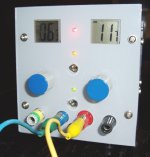
When in standby mode, the current and voltage set values are displayed.
All the components are very common, cheap and easily substitutable.
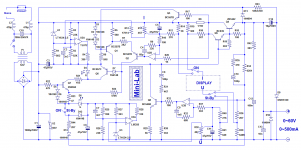
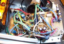
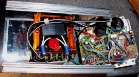
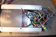
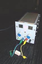
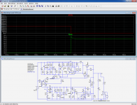
Here is the schematic that will be described later, and some pics of my finished prototype:
⚠The revised version of the schematic can be found here⚠
Here is my latest project: a small(ish) lab supply.
I already own a number of supplies, both commercial and DIY, but I felt the need for yet another one: the ones I have so far are pretty bulky things, and they have a fixed location in my lab.
- I wanted something lighter and more portable that I could move anywhere on my bench, and use like the physical dead-ringer of a spice voltage source: completely isolated, floating, agile and electrically perfect in all respects.
- Initially, I settled for a modest size: something like 40V and 200~300mA.
Then I thought it would be nice to reach a bit higher and pushed the voltage to 60V...
You can easily guess where this ended up: the usual specs creep...
The supply I finally built was three times as large as originally intended, but it still qualifies as a "small" one.
- It is a relatively traditional linear supply, with all the features you can expect for such an instrument, but it also has some unusual characteristics: it is exceptionally clean, quiet, stable and well-behaved. It also has a very minimal output bypassing, meaning the energy it can deliver to a load that is brutally shorted is absolutely minimal.
This slightly impairs the transient response, but it is always possible to temporarily add supplementary caps, whilst the opposite is impossible.
- The circuit is relatively complex, but this (moderate) complexity offers some advantages: voltage and current are variable from zero to the maximum, without the need for auxiliary supplies or similar impediments, and there is no shunt in the ground's way, meaning the circuit could very easily be used in a bipolar supply without complications.
The no-load power is also extremely low.
When in standby mode, the current and voltage set values are displayed.
All the components are very common, cheap and easily substitutable.
Here is the schematic that will be described later, and some pics of my finished prototype:
⚠The revised version of the schematic can be found here⚠
Attachments
Last edited:
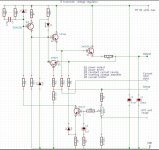
OK, let us enumerate and identify the different functions:
- The darlington Q5/Q4 is the power ballast
-Q8 is the voltage VAS and Q8 its CCS collector load
-U3B is the voltage regulator (U3A is the shunt regulator for the V control supply)
-U2B is the current regulator (U2A is the shunt regulator for the I-control supply)
-Q7 is the CCS setting the current in the shunt regulators and indicator LEDs string
The shunt regulators:
Each dual opamp uses one of its section to regulate its own supply: the inputs are connected to a bridge, of which one arm is a non-linear device, here a shunt reference.
The circuit has a strong positive feedback forcing the output to rise until the reference conducts sufficiently to change the FB to negative, thus balancing the bridge.
The output works as a shunt regulator thanks to R28 or R4 tied to one of the supply rails depending on the polarity.
Since the input voltage for the reference is derived from this very tightly regulated supply, its stability is outstanding (the circuit is somewhat incestuous).
The regulator used for the voltage control uses an opamp including GND in its input CM range, and the one for the current a type including V+ in its CMR.
The LM358 and similar is suitable for the lower side, and all biFet opamps like the TLO82 are suitable for the upper one.
In my prototype, I have upgraded to a LT1013 and LF412 for lower noise, better precision and stability.
For a negative regulator, the types would just need to be swapped (and the polarities of transistors and diodes reversed, of course).
Here is the display circuit and a sim file (it takes forever to converge, but it does converge, just be patient).
To be continued...
Attachments
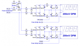
Here is the display circuit and a sim file (it takes forever to converge, but it does converge, just be patient).
Maybe you should include/attach 3rd party op amp models since .asc as is will not work.
Looking for a suitable transformer, I could only find too small ones, <200mA, which was really too small, or a larger one allowing up to 500mA.
You can easily guess where this ended up: the usual specs creep...
Don't really understand this one: what is a limitation here budget or supplier? For instance you can easily pick many 200VA+/50VAC+ toroidal transformer for the decent price on the TME.eu: i.e. 55VAC/500VA or 60VAC/400VA.
Of course if you goes over 30W cooling starts to be a big challenge without deploying some sort of pre-regulator to take most of the voltage difference between Vin and Vout.
I have included the LM358 and TL072 models, but alternatively you could use the native LT1013 (for the 358) and LT1055 (for the 72): they will probably work better than those models. The LM358 in particular is crap, it creates discontinuities and I am sure it is responsible for 80% of the convergence difficulties.Maybe you should include/attach 3rd party op amp models since .asc as is will not work.
Anyway, the sim was used mainly to study the loops stability and handover, it is not up to date or very accurate in many respects
Yes, I know I could find a transformer if I wished to, but this is DIYaudio, I do not have hard specifications to conform to, and since I have a huge stock of spare parts, I prefer to use them whenever possible.Don't really understand this one: what is a limitation here budget or supplier? For instance you can easily pick many 200VA+/50VAC+ toroidal transformer for the decent price on the TME.eu: i.e. 55VAC/500VA or 60VAC/400VA.
Of course if you goes over 30W cooling starts to be a big challenge without deploying some sort of pre-regulator to take most of the voltage difference between Vin and Vout.
For my paid work, I have a completely different point of view, but this is a hobby and I adopt a relaxed attitude.
Voltage regulator:
U3B compares the set voltage from the V potentiometer to an image of the output voltage scaled by R34/R36-R39, and drives the voltage amplifier/translator Q8 accordingly.
The resulting voltage drives the power follower Q5-Q4.
When in voltage mode, Q2 is inactive and Q1 provides a pull-up current of ~2mA.
Both the reference and feedback voltages undergo an additional scaling ending up at 1/1000th of the output voltage, to drive the panel-meter.
The various RC networks provide the compensations of the loop.
When the standby switch is closed, D13 and R44 force a voltage higher than any possible reference on the FB input, thus in effect shutting down the regulator. It also shorts the green "ON" LED via D12.
D10 protects the output against reverse voltages, if for example the supply is associated with others.
D11 provides load-dumping protection. Short duration events are absorbed by the filter cap C1, and if the situation lasts, U2 (60V AC, ~85V DC) clamps the voltage to a safe value.
Attachments

Here they are:
.MODEL BD243A NPN(IS=3.11126E-13 ISE=6.90683E-11 ISC=3.31131E-13 XTI=3 BF=93.0 BR=9.78891 IKF=5.62341 IKR=0.0382066 XTB=1.9711 VAF=174.5 VAR=122.381 VJE=0.6403992 VJC=0.4308133 RE=0.701391 RC=0.701391 RB=43.8404 RBM=0.436865 IRB=5.2264E-5 CJE=8.001919E-10 CJC=1.34699E-10 XCJC=0.5559 FC=0.5 NF=0.973751 NR=0.980115 NE=2.0 NC=1.09387 MJE=0.339666 MJC=0.347066 EG=1.2325 KF=1E-9 AF=1 VCEO=60 ICRATING=3 MFG=FAIRCHILD)
.MODEL BD139 NPN(IS=1e-09 BF=222.664 NF=0.85 VAF=36.4079 IKF=0.166126 ISE=5.03418e-09 NE=1.45313 BR=1.35467 NR=1.33751 VAR=142.931 IKR=1.66126 ISC=5.02557e-09 NC=3.10227 RB=26.9143 IRB=0.1 RBM=0.1 RE=0.000472454 RC=1.04109 XTB=0.727762 XTI=1.04311 EG=1.05 CJE=1e-11 VJE=0.75 MJE=0.33 TF=1e-09 XTF=1 VTF=10 ITF=0.01 CJC=1e-11 VJC=0.75 MJC=0.33 XCJC=0.9 FC=0.5 CJS=0 VJS=0.75 MJS=0.5 TR=1e-07 PTF=0 KF=0 AF=1¸ VCEO=80 ICRATING=1A MFG=PHILIPS)
Note that you could probably use any similar transistors you have available as models, and anyway, the real circuit uses different types too.
When you need models, I recommend you visit the LIB section of the Yahoo group, most of them are available there:
https://groups.yahoo.com/neo/groups/LTspice/files/ Lib/
Current regulator:
When the voltage across the current shunt R8 exceeds the value set by the potentiometer R11, U2B "steals" current from Q1 through R7 and the B-E diode of Q2, thus taking control of the output current.
Since Q2 is also heavily saturated, it pulls D7 and R24, removing the base current from Q6, and allowing the string current to pass through the current indicator LED D4.
The shunt and reference voltages are also scaled, like in the voltage section, to drive the panel meter.
C4 and R8 compensate the loop.
In addition to the main current servo loop, there is also a simpler, fast path, feedforward circuit: when the voltage across the shunt exceeds ~0.6V, Q3 conducts and blocks the base bias of Q1.
Since this circuit is very fast, it means that the current will always be limited to ~<600mA, even for transient conditions.
The "normal" regulation path through the opamp has a delay of tens or hundreds ns, and in the case of a very brutal short at the output, this would allow a transient current spike in the load and the ballast transistor.
The output is also equipped with a snubber circuit composed of R43, C14 and D9.
When the supply operates in current mode and the load is brutally removed, the voltage loop needs some time to "wake up" and regain control of the output voltage. This results in a transient overvoltage at the output, and this could damage sensitive loads.
There are a number of ways to tackle this issue:
The fast diode D9 is always kept on the verge of conduction thanks to R43, and as soon as a spike appears, it conducts fully and clips it.
With this uncomplicated circuit, the maximum overshoot is kept well under a few hundreds mV, perfectly safe even for delicate circuits.
When the voltage across the current shunt R8 exceeds the value set by the potentiometer R11, U2B "steals" current from Q1 through R7 and the B-E diode of Q2, thus taking control of the output current.
Since Q2 is also heavily saturated, it pulls D7 and R24, removing the base current from Q6, and allowing the string current to pass through the current indicator LED D4.
The shunt and reference voltages are also scaled, like in the voltage section, to drive the panel meter.
C4 and R8 compensate the loop.
In addition to the main current servo loop, there is also a simpler, fast path, feedforward circuit: when the voltage across the shunt exceeds ~0.6V, Q3 conducts and blocks the base bias of Q1.
Since this circuit is very fast, it means that the current will always be limited to ~<600mA, even for transient conditions.
The "normal" regulation path through the opamp has a delay of tens or hundreds ns, and in the case of a very brutal short at the output, this would allow a transient current spike in the load and the ballast transistor.
The output is also equipped with a snubber circuit composed of R43, C14 and D9.
When the supply operates in current mode and the load is brutally removed, the voltage loop needs some time to "wake up" and regain control of the output voltage. This results in a transient overvoltage at the output, and this could damage sensitive loads.
There are a number of ways to tackle this issue:
- The simplest and most commonly used is to increase the output capacitance to a large value, 10µF or more.
This leaves the V loop enough time to regain control without overshoot, but of course it also increases the energy stored by the supply, energy that can be delivered in uncontrolled manner if the load becomes shorted: a 10µF cap charged at 60V stores enough energy to damage almost any semiconductor component, even large ones. - Another possibility is to keep both loops always active in linear regime, so that the transition from one to the other is instantaneous and seamless, but it seriously complicates the circuitry.
- Finally, the issue can also be solved by a 2 quadrant output stage, but it also complicates matters and requires an additional power element.
The fast diode D9 is always kept on the verge of conduction thanks to R43, and as soon as a spike appears, it conducts fully and clips it.
With this uncomplicated circuit, the maximum overshoot is kept well under a few hundreds mV, perfectly safe even for delicate circuits.
Display:
The display uses miniature millivoltmeter modules cannibalized from small battery testers.
I found them for very cheap, and when I discovered the millivoltmeter was usable on its own, I bought the whole stock.
The modules are so small I can sneak them nearly anywhere I like.
They are also very low power: they need less than 1mA/3V.
Their operation is very much like the common DPM's operating on 9V, except all the voltages are 3 times smaller. In particular, they also need a floating supply with respect to the input ground.
Here, that requirement is fulfilled by a special arrangement of capacitive supply, meaning there is no need for additional transformers or windings.
The voltage is stabilized to ~3V by two red LED in series.
Exactly the same circuit could be used with regular 9V DPM's: one just needs to replace the LEDs by a single 9.1V zener.
The capacitive currents from the two supplies also serve to power the mains LED, thus giving an instant ON/OFF indication, just like an old neon pilot light.
Miscellaneous:
For a maximum of flexibility, I have used a particular scheme of earthing/grounding: basically, the supply is built as a class 2 device and wouldn't require a protective earth. The output is completely floating.
Nevertheless, the power cord brings the earth to the supply, but it isn't permanently connected to anything, it is simply made accessible from the front panel. The chassis is also floating and accessible, as is the transformer screen.
This allows me to chose the best-suited configuration for any application: I could connect the earth to the transformer screen and the chassis to the ground of the DUT to minimize hum pick-up for example, or if I would like to replace the Vbe multiplier of an amplifier by this supply for investigation purposes, I would leave the output floating, and use the screen and chassis as a guard connected to the output of the amplifier to minimize capacitive effects.
The supply has a basic mains filter, working for differential and common-mode, but of course no "Y" capacitors anywhere, the plague of so many equipments.
The transformer itself is of the regular EI variety, to minimize primary to secondary capacitance.
Note that the topology used in this supply can very easily be adapted to other voltage/current combinations: you just need to modify two or three resistor values, and select transistors capable of handling the desired voltage/current/power.
The polarity can be reversed by changing the sex of all transistors, and swapping the LM358 and TL072
Here they are:
.MODEL BD243A NPN(IS=3.11126E-13 ISE=6.90683E-11 ISC=3.31131E-13 XTI=3 BF=93.0 BR=9.78891 IKF=5.62341 IKR=0.0382066 XTB=1.9711 VAF=174.5 VAR=122.381 VJE=0.6403992 VJC=0.4308133 RE=0.701391 RC=0.701391 RB=43.8404 RBM=0.436865 IRB=5.2264E-5 CJE=8.001919E-10 CJC=1.34699E-10 XCJC=0.5559 FC=0.5 NF=0.973751 NR=0.980115 NE=2.0 NC=1.09387 MJE=0.339666 MJC=0.347066 EG=1.2325 KF=1E-9 AF=1 VCEO=60 ICRATING=3 MFG=FAIRCHILD)
.MODEL BD139 NPN(IS=1e-09 BF=222.664 NF=0.85 VAF=36.4079 IKF=0.166126 ISE=5.03418e-09 NE=1.45313 BR=1.35467 NR=1.33751 VAR=142.931 IKR=1.66126 ISC=5.02557e-09 NC=3.10227 RB=26.9143 IRB=0.1 RBM=0.1 RE=0.000472454 RC=1.04109 XTB=0.727762 XTI=1.04311 EG=1.05 CJE=1e-11 VJE=0.75 MJE=0.33 TF=1e-09 XTF=1 VTF=10 ITF=0.01 CJC=1e-11 VJC=0.75 MJC=0.33 XCJC=0.9 FC=0.5 CJS=0 VJS=0.75 MJS=0.5 TR=1e-07 PTF=0 KF=0 AF=1¸ VCEO=80 ICRATING=1A MFG=PHILIPS)
Note that you could probably use any similar transistors you have available as models, and anyway, the real circuit uses different types too.
When you need models, I recommend you visit the LIB section of the Yahoo group, most of them are available there:
https://groups.yahoo.com/neo/groups/LTspice/files/ Lib/
Tested with changing voltage and it looks pretty nice. For some reason I didn't succeed to limit a current playing with R33, R34. Tested model is in the attachment.
Attachments
For some reason, Windows doesn't want to unzip your files. I also tried an online unzipper, but it doesn't work either:
You can post your .asc directly, if there are not too exotic models to add, I'll manageSorry, an error occurred while processing your request.
In the mean time, I made checks with the substitutions I advised you as a quick fix for the lack of models, and there seems to be a problem with the LT1055 in that configuration: it behaves in unexpected ways, and this disables the current regulator.
It is probably preferable to use the TL072 model I provided: it works as expected and doesn't cause any convergence issue, contrary to the LM358 for which the LT1013 is a good substitute, both in sim and reality.
It is probably preferable to use the TL072 model I provided: it works as expected and doesn't cause any convergence issue, contrary to the LM358 for which the LT1013 is a good substitute, both in sim and reality.
For some reason, Windows doesn't want to unzip your files. I also tried an online unzipper, but it doesn't work either:
You can post your .asc directly, if there are not too exotic models to add, I'll manage
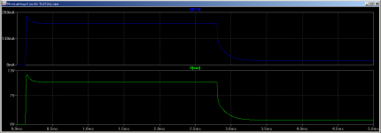
Strange, maybe its due to fact that one file has linux owner rights recorded. Here is another one, this time also with TL072 as you suggested. Yes, current limitation now works and it produce overshoot (~15% in tested case).
Attachments
Elvee, I also have another question: what is a benefit of using two voltage reference? Is that in anyway connected with some limitation of choosen LT1634?
Probably because they don't share same ground.
Frex
Probably because they don't share same ground.
Frex
Too obvious

Thanks Frex
The situation you examine there is that of a step at the reference input, ie. the regulator functionning as an amplifier.Yes, current limitation now works and it produce overshoot (~15% in tested case).
It can be interesting for the study of some parameters, but it isn't a likely realistic situation with the potentiometer control and the 47µ bypass.
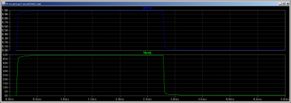
A stimulus applied at the output is normally what is encountered, and if it results in a change from current-mode to voltage-mode, an overshoot will result, as shown in the sim and screenshot below.
This is why the snubber network is included.
Elvee, I also have another question: what is a benefit of using two voltage reference? Is that in anyway connected with some limitation of choosen LT1634?
That is the reason, of course. It is one of my regrets, but choices are to be made, and since I didn't want to place the current shunt in the ground line, this left two options: the non-regulated input and the output.Probably because they don't share same ground.
Frex
None share a common ground with the voltage control circuit, and the output being variable, this complicates things more than at the input.
If a remote or µcontroller control was desired, it would be possible to translate/ rapatriate the control to the ground, but it would add a layer of complication and inaccuracies, and since I just needed the manual control, I simply used two different reference potentials and two reference circuits.
Not the most elegant of solutions, I agree.
One thing worth noting regarding the current control: all Bifet opamps (probably including the real LT1055) include V+ in their common mode voltage range: it is clearly stated in the datasheet, but it is not reflected in the numerical values of the DS.
This is in fact means that the basic operation is guaranteed, but not the specifications. The OL gain in particular is reduced.
There are series (TLOX IIRC) for which the characteristics are guaranteed, but they are less common (and more expensive).
Attachments
The situation you examine there is that of a step at the reference input, ie. the regulator functionning as an amplifier.
It can be interesting for the study of some parameters, but it isn't a likely realistic situation with the potentiometer control and the 47µ bypass.
You're right. I used it as a special case to see what could happened when PSU is controlled by MCU. But as you also mentioned due to current control loop your design is not "MCU ready" what is just fine if one don't need anything beyond basic manual settings.
- Status
- This old topic is closed. If you want to reopen this topic, contact a moderator using the "Report Post" button.
- Home
- Design & Build
- Equipment & Tools
- Mini-Lab Supply