Hello,
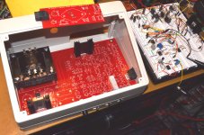
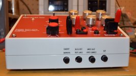
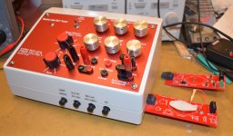
Well winter has come early this year, so I got serious about finally constructing my semiconductor tester for BJT, Mosfets, JFets and D-Mosfets. Many projects are waiting for match sets. I have an eBay tester, but I do wonder about it, unless I really have a MJ15003 with 450 hFE. Here is a picture of the case and PCB with the old transformer I bought about a hundred years ago. I will run a few more test on the prototype pictured next to the case. Probably could of got an old heath kit off eBay for less, but where is the fun in that.
Later,
MI
Attachments
High Power Version
Before this one is finished. I have an idea about a higher powered simplified version, maybe 4-5 A max, probably no manual sweep, too most dissipation to deal with. IXYS makes some 16A depletion mode mosfets. I have a 40 VCT 200VA toroid, +/- 28vDC. Need to figure out how to heat sink TO-3, TO-3P, TO-247, etc. with DUT quick replace/repeat ability, probably an ungrounded floating heat sink. Test only power BJT, Mosfets both vertical and lateral.
MI
Hi MadInventor,
Can you tell us more about your invention? It appears to be a curve tracer, or is it? How do you go about using it and what do you test for?
As you should know, beta is extremely temperature dependant. You pretty much have to specify current level and case temperature along with the beta value you quote if you want to be accurate.
Anyway, enough that you created a pretty cool looking piece of equipment. How about writing a manual for it? Are you going to make the project available for others to build, or will you be selling them?
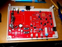
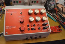
Anyway, excellent workmanship and case design from the looks of it. More pictures from front and side on? How about some pictures of the completed PCB?
-Chris
Can you tell us more about your invention? It appears to be a curve tracer, or is it? How do you go about using it and what do you test for?
As you should know, beta is extremely temperature dependant. You pretty much have to specify current level and case temperature along with the beta value you quote if you want to be accurate.
Anyway, enough that you created a pretty cool looking piece of equipment. How about writing a manual for it? Are you going to make the project available for others to build, or will you be selling them?
Anyway, excellent workmanship and case design from the looks of it. More pictures from front and side on? How about some pictures of the completed PCB?
-Chris
SD Tester
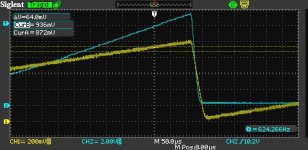
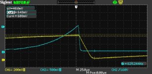
Yes and no. I can run it in XY mode on scope, but not what I intended, below is a image of a 2SK1058, set for 100mA drain current(blue) and Vgs (yellow) range set by cursors. I was looking more for a solution to IPS current points, forward voltages, OPS bias current, depletion mosfet CCS and obviously matching. I did include base/collector current test points for beta calculations. If I did it over I would have four base resistors (10, 100, 1K, 10K). Tester can be ran in sweep or manual, sweep for sorting and manual for more accurate measurements.
The DUT Power switch was changed to up - leave on, cover over device, with temperature readings, center - off, down - on momentary - read quickly, device at "room temperature".
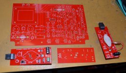
No, I won't be selling the tester, if anyone wants to build one, they can. I have extra PCBs if anyone is interested, but they were made for a transformer I have had for along time. Different ones could be mounted in place of the one I used, 36VAC CT(2 x 18) @500mA or more.
Thanks for the kind words!
The panel was made by Front Panel Express. The case is a BUD box. I marked some holes wrong for the push buttons, had to elongate them. I might add more pictures later.
Thanks,
MI
Can you tell us more about your invention? It appears to be a curve tracer, or is it? How do you go about using it and what do you test for?
Yes and no. I can run it in XY mode on scope, but not what I intended, below is a image of a 2SK1058, set for 100mA drain current(blue) and Vgs (yellow) range set by cursors. I was looking more for a solution to IPS current points, forward voltages, OPS bias current, depletion mosfet CCS and obviously matching. I did include base/collector current test points for beta calculations. If I did it over I would have four base resistors (10, 100, 1K, 10K). Tester can be ran in sweep or manual, sweep for sorting and manual for more accurate measurements.
As you should know, beta is extremely temperature dependant. You pretty much have to specify current level and case temperature along with the beta value you quote if you want to be accurate.
The DUT Power switch was changed to up - leave on, cover over device, with temperature readings, center - off, down - on momentary - read quickly, device at "room temperature".
Anyway, enough that you created a pretty cool looking piece of equipment. How about writing a manual for it? Are you going to make the project available for others to build, or will you be selling them?
No, I won't be selling the tester, if anyone wants to build one, they can. I have extra PCBs if anyone is interested, but they were made for a transformer I have had for along time. Different ones could be mounted in place of the one I used, 36VAC CT(2 x 18) @500mA or more.
Anyway, excellent workmanship and case design from the looks of it. More pictures from front and side on? How about some pictures of the completed PCB?
Thanks for the kind words!
The panel was made by Front Panel Express. The case is a BUD box. I marked some holes wrong for the push buttons, had to elongate them. I might add more pictures later.
Thanks,
MI
Attachments
It's good stuff MI, that we could use also.
Thanks for making and sharing it.
So I take it the boards are for the original and not
the V1 R2 version of it?
I'd be interested in the boards and additional pics.
Looks like a good project and useful too.
How much better is V1 R2, as the Mosfet drive is not unclamped?
That is better for? Ok, got it. If clamped, then you can't work
the mosfet as "hard" so how would you test the higher current points?
Hence, non-clamped.
cheers,
Last edited:
SD-Tester
You're welcome, the pcbs have one trace that needs to be cut. This allows depletion mode mosfet gates to be driven to 8 volts(Vgs) which is max., bjt and jfets are clamped at 1.2 volts. The pushbuttons set up the devices for drive polarity. So that everyone knows, these boards contain lead, I got them from PCBway and forgot to check HASL lead free, my mistake. Here are some more images, the scope trace is a MPS8099 where collector current is set at 1.6 mA and matching Vf between cursors, for my Leach amp.
MI
It's good stuff MI, that we could use also.
Thanks for making and sharing it.
So I take it the boards are for the original and not
the V1 R2 version of it?
I'd be interested in the boards and additional pics.
Looks like a good project and useful too.
How much better is V1 R2, as the Mosfet drive is not unclamped?
That is better for? Ok, got it. If clamped, then you can't work
the mosfet as "hard" so how would you test the higher current points?
Hence, non-clamped.
cheers,
You're welcome, the pcbs have one trace that needs to be cut. This allows depletion mode mosfet gates to be driven to 8 volts(Vgs) which is max., bjt and jfets are clamped at 1.2 volts. The pushbuttons set up the devices for drive polarity. So that everyone knows, these boards contain lead, I got them from PCBway and forgot to check HASL lead free, my mistake. Here are some more images, the scope trace is a MPS8099 where collector current is set at 1.6 mA and matching Vf between cursors, for my Leach amp.
MI
Attachments
Its hard to get all the functionality into one system.
That is one reason why I'm looking at a higher current version for power devices.
MI
The problem with high current is that you generate heat everywhere. Connections become very important and voltage drops generated by the high current are big sources of error. This is true even if the test is a pulse type (except heat is less of an issue).
-Chris
Chris,
Like they say in the movies, I got to try. Found a 300 mA buffer for drive and a high voltage opamp. Probably will not use DMosfet current limiting, resistor plus fuse instead. Will tailor for 2-2.5 A max. .25 A/V current sense. Have an idea about mounting heatsink with TO-3 and terminal block for TO-3P-247 on top of pcb and configure with jumpers instead of switches.
MI
- Status
- This old topic is closed. If you want to reopen this topic, contact a moderator using the "Report Post" button.
- Home
- Design & Build
- Equipment & Tools
- Started My Transistor Tester