
U3 substitutes and spares
first of all I´d like to thank underwurld for sharing his work results.
I just bricked my SI-9000 (THT version) by accidently applying 30V revers voltage to the output when calibrating it :-(
The output buffer OP amp (U3) had gone. As the code had been sanded off and the part has quite some demanding specs, a suited spare wasn’t easy to find.
Some types mentioned in this forum (AD797, etc.) won´t probably work, because they use V+ instead of V- referenced offset adjustment.
After spending some time investigating, I figured out these typed:
AD817
AD847
LM6361
LT1357
LT1360
LT1363
All of these have at least 25 MHz bandwidth, 300V/µs slewrate and low noise. I will give the LT1360 a try because it´s availability and price (about 4 EUR/1) and its excellent specs.
In the meanwhile, I run the SI-9000 with a TL081 (crappy 100 kHz bandwidth)")
first of all I´d like to thank underwurld for sharing his work results.
I just bricked my SI-9000 (THT version) by accidently applying 30V revers voltage to the output when calibrating it :-(
The output buffer OP amp (U3) had gone. As the code had been sanded off and the part has quite some demanding specs, a suited spare wasn’t easy to find.
Some types mentioned in this forum (AD797, etc.) won´t probably work, because they use V+ instead of V- referenced offset adjustment.
After spending some time investigating, I figured out these typed:
AD817
AD847
LM6361
LT1357
LT1360
LT1363
All of these have at least 25 MHz bandwidth, 300V/µs slewrate and low noise. I will give the LT1360 a try because it´s availability and price (about 4 EUR/1) and its excellent specs.
In the meanwhile, I run the SI-9000 with a TL081 (crappy 100 kHz bandwidth)
Hello I write from Italy, you very good great job reverse engineering.
probe power supply be your creation or integrated probe?
I can feed with different dual power supply 9v battery 500mah
resistors marked point have tolerance 1%?
What power Watts have resistances this circuit?
You can publish original probe picture layout component
probe power supply be your creation or integrated probe?
I can feed with different dual power supply 9v battery 500mah
resistors marked point have tolerance 1%?
What power Watts have resistances this circuit?
You can publish original probe picture layout component
@underwurlde : Great post!
Perhaps adding a photo of other PCB side and how compensating capacitor are arranged (under resistor divider) would make even more clearer (if your device is still apart).
I took a look on schematics SMD type, but I think that R40 is somehow positioned in wrong way. I have searched many current mirrors, Wilson, Widlar,...any current mirror that exists, and haven't found any such mirror that has a resistor in that place.
The listed components are quite old and difficult to find. The U441 is now produced by Linear Systems. I wish I could understand the principles of the weird pair jfet + bjt.
Underwurlde,
Can you attach your pics now lost from posts 1 & 2?
@underwurlde Thank very much for the trouble. Great value!
I would also find the pictures very useful!
I appreciate your work. I think most of these (even the Tek and Agilent ones) are made by a vendor in Taiwan. I met them at a trade show in Taipei years ago and they seemed pretty serious and responsible. I would caution against making a copy China style. Make sure you understand the function of each element first (I'm sure this goes without saying) since the high voltages involved are really dangerous. Even the spacing between traces can be an issue, especially with fast rise HV pulses.
The basic FET buffer into an IC makes a lot of sense. It would not work at 20 MHz without a much more complex divider. I have a couple of Pomona branded versions that I look inside of. The potential of upgrading the opamp is interesting.
Hello 1audio! Could you elaborate on the voltage divider? What are you main concerns? Parasitics?
Aiming at a much higher frequency, say around 1 GHz, what would you consider for a high quality design?
Any idea what goes inside a branded one, ie: N2793A 800 MHz 10:1 Differential Probe | Keysight (formerly Agilent’s Electronic Measurement)
It seems to be a quite different approach. Starting with the 200 kΩ//1 pF between inputs. Of course the tips also play a role here, but apart that, any news about someone rev. engineering one of those?
The FET bipolar part makes sense, high current gain and low capacitance at the input is critical to getting a high impedance input. good matching of the two buffers helps and the CMRR trim is important. Most of the CMRR comes from the opamp.
The resistors have 2200 pF in parallel? The ratio is roughly 200:1 I think and that would suggest an input cap of around 1 uF. Perhaps those are 2.2 pF HV caps? That would make more sense.
Opamp selection for this would entail understanding the frequency range its supposed to operate over. A 741 would not have enough bandwidth to be very useful. There are a number of new opamps that could give as much as 100 MHz from it, however the rest of the circuit would not be up to the task.
There is a lot to be learned from studying the Tek plugins and probes. Many of the manuals can be found on the web for free.
I am not sure about the 2200 pF in parallel... Checking the SMT version, reducing impedances to Zth, it seems like this: (just front end)

AC sweep analysis with 1V gives:

C3 and C7 are the variable capacitors.
At DC, ratio is ~ 150:1.
That seems odd for a 25 MHz spec. What am I missing?
In case anyone wants to fuss over the simulation files (ltspice). I have also included the poti123 symbol and sub. It came from the yahoo group, credits to Helmut, I guess
View attachment Differential probe - front end simulation.asc
View attachment Poti123.zip
> odd for a 25 MHz spec
C2 C3 against ~~26K is 9.6KHz, essentially as your graph says.
Counting on thumbs, C1 times 150 means C2 C3 and Silicon should be 450pFd. I see 325pFd. It seems unlikely the Silicon adds 125pFd. I think C2 could be bigger, and trimmable. Specially since C1 will have large uncertainty being so small.
After spending some time investigating, I figured out these typed:
AD817
AD847
LM6361
LT1357
LT1360
LT1363
All of these have at least 25 MHz bandwidth, 300V/µs slewrate and low noise. I will give the LT1360 a try because it´s availability and price (about 4 EUR/1) and its excellent specs.
In the meanwhile, I run the SI-9000 with a TL081 (crappy 100 kHz bandwidth)
I would add also the LM7171 to the list.
Hello. Sorry for resurrecting old topic. I would like to know what is the purpose of the capacitors in the input resistor divider stage. Are they there to filter some noise? Are they needed at all? Do they limit the bandwith of the probe, and how to calculate that? Thank you in advance.
OK. As I understand, the capacitors are used for compensating the parasitic capacitance of the resistors. The parasitic capacitance is low, so adding parallel capacitors is making the parasitic capacitance negligable comared ot the capacitance of the added capacitors?
And the ratio of the capacitance in the divider has to have the same ratio as resistors (1/100 if the resistor divider is 1/100). But, how do I know what values to use (for parallel caps on the resistors)? I should use the smallest possible values, right? To have the lowest possible input capacitance of the probe?
How do I calculate the values of capacitors, in order to have a divider bandwith of around 200 MHz?
I was doing some simulations in TI Tina, and my input divider stage dos not attenuate the signal amplitude at all regardless of the frequency (tried 200 MHz max).
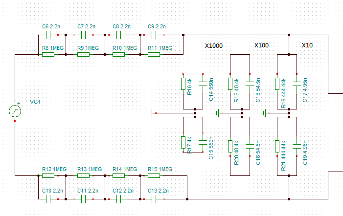
I thought that the input divider will act as a low pass filter, and limmit the bandwith. If it does, how can I simulate that?
I thought that the input divider will act as a low pass filter, and limmit the bandwith. If it does, how can I simulate that?
Hello. Sorry for resurrecting old topic. I would like to know what is the purpose of the capacitors in the input resistor divider stage. Are they there to filter some noise? Are they needed at all? Do they limit the bandwith of the probe, and how to calculate that? Thank you in advance.
OK. As I understand, the capacitors are used for compensating the parasitic capacitance of the resistors. The parasitic capacitance is low, so adding parallel capacitors is making the parasitic capacitance negligable comared ot the capacitance of the added capacitors?
And the ratio of the capacitance in the divider has to have the same ratio as resistors (1/100 if the resistor divider is 1/100). But, how do I know what values to use (for parallel caps on the resistors)? I should use the smallest possible values, right? To have the lowest possible input capacitance of the probe?
How do I calculate the values of capacitors, in order to have a divider bandwith of around 200 MHz?
The idea is to make the attenuation for higher freq the same as for low frequency. The parasitic capacitance of the series R will make the series R look smaller at higher frequencies so the attenuation becomes less, you get peaking.
To try out, change all the caps on each resistor to a realistic parasitic cap value like 2 or 3pF (your 2.2n is way out of range). Depending on your physical layout, you may need to add also small parasitics from the 1st resistor to the last, etc.
Then check the freq response, you will see that the response rises at higher frequencies. Now start to increase caps to the resistors to ground, until you have the flattest response.
Jan
Thanks for the reply.
The caps on the schematics are actually physical caps, not the parasitic. I wanted to see if it will work like that, because if the parasicit capacitance is 2-3pF, then 1000 times higher capacitance in parallel (2.2nF) means that I don't need to worry about the parasitics, just the physical capacitence.
I will do what you suggested, and see what happens.
Now I have more problems in how to increase the bandwith of the instrumentional amplifier section (made of 3 identical opamps, all set to gain of 1). Because instead of around 200MHz unity gain bandwith, I get about 120 MHz or so (-3dB). I have to find out / learn how the passive components (resistors and capacitors) in opamp circuit influence its bandwith.
- Home
- Design & Build
- Equipment & Tools
- Differential Probe - Reverese Engineered