I suggest the first kick at the can would be to build the simpler, single AK5388 mono-design shown in Fig.1 of the app note. It has a simple mux for the output and puts off the fussy FGPA work until later.
It would allow the creation/testing of the analog input stages , clocks and power supplies. The output of the card would be plain vanillia I2S. Theoretically the card should be able to mate with any I2S engine, commercial or open-source.
George
Hi George,
Yes the idea is for the card to able to mate to any I2S. I would like it to be stand alone if possible. I would prefer what ever technology is used is in a form I can work with and have access to. And if someone else wants to dig into it for there own purpose they are quite welcome to. There is nothing more frustrating to a DIY to be dependent on someone else for up grades or a certain amount of interest just get to a board. After all it's DIY.
Cheers,
Last edited:
I have the AKD5394a board and could connect it to the audiowidget board. I would be happy to try it. I need some insight as to which pins on the the module to connect to get it running? The demo board has oscillators and dividers so the necessary clocks and data are available. Do I need to connect I2C? The I2S connections should be pretty straightforward.
I can easily graft different Input circuits. I'll use the QA400 interface board as a starting point to try things.
I can easily graft different Input circuits. I'll use the QA400 interface board as a starting point to try things.
I have the AKD5394a board and could connect it to the audiowidget board. I would be happy to try it. I need some insight as to which pins on the the module to connect to get it running? The demo board has oscillators and dividers so the necessary clocks and data are available. Do I need to connect I2C? The I2S connections should be pretty straightforward.
I can easily graft different Input circuits. I'll use the QA400 interface board as a starting point to try things.
You can pull up the connection I/O for Borge's boards on his site at Q N K T C USB-I2S Module and Analog Board
However, I do not believe the firmware for the Audio-Widget supports ADC input. ( I could be wrong )
George
Hi Demian,
does your board run out of the box in some recognizeable mode? If you don't need to do an awful lot of configuration, leave the I2C.
Assuming you're using an AB-1.2 class thingy to start with: MCLK-wise I'd recommend you to tap MCLK from the AB-1.2 and patch it into the AK board. The USB-I2S module receives clock commands from the PC. You can choose 2x.xxMHz at the XOs or a 2^n division at the dividers you so wisely had me put in")
Alternatlively, you can change the USB descriptors to only reflect the sample rates your AK board operates on. Then you'd need to send MCLK in the opposite direction. There should be plenty of places where you can strap things in on the AB-1.2.
Let me know which HW you start out with on the USB side of things, and I can try to give you some patching guidance.
Børge
does your board run out of the box in some recognizeable mode? If you don't need to do an awful lot of configuration, leave the I2C.
Assuming you're using an AB-1.2 class thingy to start with: MCLK-wise I'd recommend you to tap MCLK from the AB-1.2 and patch it into the AK board. The USB-I2S module receives clock commands from the PC. You can choose 2x.xxMHz at the XOs or a 2^n division at the dividers you so wisely had me put in
Alternatlively, you can change the USB descriptors to only reflect the sample rates your AK board operates on. Then you'd need to send MCLK in the opposite direction. There should be plenty of places where you can strap things in on the AB-1.2.
Let me know which HW you start out with on the USB side of things, and I can try to give you some patching guidance.
Børge
George, you are right, the audio-widget branch of the firmware does not support the ADC.
The ADC is selectable through WidgetControl. One option is to add ADC functionality from the SDR-widget branch into the audio-widget branch, and use the WidgetControl setting (or a Makefile define) to maintain DAC-only compatibility. Unfortunately, I'm not the guy to do that coding work just now.
Børge
George, you are right, the audio-widget branch of the firmware does not support the ADC.
The ADC is selectable through WidgetControl. One option is to add ADC functionality from the SDR-widget branch into the audio-widget branch, and use the WidgetControl setting (or a Makefile define) to maintain DAC-only compatibility. Unfortunately, I'm not the guy to do that coding work just now.
Børge
Porting the ADC component of the SDR-Widget to the Audio-Widget is not trivial. The SDR-Widget AK5394A card is tightly coupled to the Atmel processor and does more than support the I2S signal. All of the ADC sample-rate, calibration etc is driven or monitored by the cpu. To turn the Audio-Widget into a pure I2S slave, AK5394 code is set for master mode, you would need to hack quite of code.
Demian, grab the SDR-Widget document archive for the schematics on how the ADC is set up.
George
I'll dig into that later this week. I have an extra audio widget (AB1.2?) module that I got from Borge some time ago for this project. I had a sense it would not be as simple as connecting a few wires. However it seems its not as onerous as it might be.
The AKM demo board has the I2S breakout and the other connections to enable a quick patch to test all of this. I have really not used the audio widget on Windows yet so that is a separate task for me. How different is the SDR widget code from the audio widget? To use the SDR widget code what needs to be done in broad terms?
The AKM demo board has the I2S breakout and the other connections to enable a quick patch to test all of this. I have really not used the audio widget on Windows yet so that is a separate task for me. How different is the SDR widget code from the audio widget? To use the SDR widget code what needs to be done in broad terms?
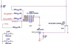
A quick summary of what I need to do to connect the AKD5394a to the QNKTC I2S module (I think):
1) Connect I2S lines at follows:
TP62 to port 3 pin 3 (L/R clk)
TP62 to port 3 pin 2 (Bit clock)
TP60 to port 3 pin 4 (Data)
TP36 to port 3 pin 1 (mclk at 12 MHz)
I will leave the board fixed at 192 KHz. (I presume that bit clock and L/R clocks are outputs from QNKTC)
What do I need to do to get a firmware that will run this and something that Windows will recognize as an audio source? (Hacked driver??)
Attached are clips from the documents for my reference as much as anything.
Attachments
I would use a probe concept to manage different applications and dynamic requirements. Making it autorange etc with protection against overload, really low internal noise etc. is way more complex than the device itself. AC coupling at the input makes sense and differential attenuator probes can handle voltage issues. Easily swapped for direct input probes for low level signals.
I have designed most of the necessary protection stuff and its more real estate than the circuit itself. That's why I abandoned that approach. I can dig it out if there is interest.
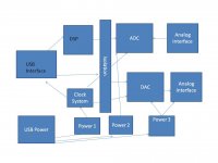
For the purposes of discussion here is a really crude block diagram of the components of a system.
A few notes on the diagram-
1) USB power, this enables running entirely from the batteries on a laptop, eliminating AC noise issues. We may need two USB power sources to support everything. We can probably only count on 2.5W per USB connection.
2) DAC and ADC isolated from each other, again eliminating common ground noise issues.
3) Master clock isolated as well and transformer coupled, this does a good job of keeping loading and power noise from affecting the jitter of the oscillators
4) I show a block for DSP for mixing multiple ADC's. For realtime stuff, like recording, this may be useful for improving the system. For measurements we can use averaging schemes to do something similar, possibly.
5) We will probably need I2S controls to both the ADC and the DAC.
Its conceivable that we could add autoranging and use the host micro to manage it and report back to the PC the current gain ranges etc. However then the PC application would need to manage the info. It can get out of hand really quick. See above.
If we break it down then the blocks can be addressed individually making the project less overwhelming. I'll post what I have done so far when I find it all.
Its quite possible to dump parts of this but in the long run limitations will arise.
This won't be real cheap to build. But the performance would potentially be on a par with the best commercial stuff.
Input and output levels-
I would go for a fixed output of 3V RMS max, again a passive attenuator can scale it down and 3V should drive any typical amplifier to clipping.
Input of 3V RMS which is close to the actual differential input limit for the chip. Adding a preamp of 40 dB will extend the low level of the system. I figure a practical noise floor of 100 Ohms equivalent (1.2 nV/rtHz) would be the limit and 40 dB of gain will move the preamp noise floor approx 15 dB above the ADC. 40 dB is nice for arithmetic but other settings are an option.
Comments?
I have designed most of the necessary protection stuff and its more real estate than the circuit itself. That's why I abandoned that approach. I can dig it out if there is interest.
For the purposes of discussion here is a really crude block diagram of the components of a system.
A few notes on the diagram-
1) USB power, this enables running entirely from the batteries on a laptop, eliminating AC noise issues. We may need two USB power sources to support everything. We can probably only count on 2.5W per USB connection.
2) DAC and ADC isolated from each other, again eliminating common ground noise issues.
3) Master clock isolated as well and transformer coupled, this does a good job of keeping loading and power noise from affecting the jitter of the oscillators
4) I show a block for DSP for mixing multiple ADC's. For realtime stuff, like recording, this may be useful for improving the system. For measurements we can use averaging schemes to do something similar, possibly.
5) We will probably need I2S controls to both the ADC and the DAC.
Its conceivable that we could add autoranging and use the host micro to manage it and report back to the PC the current gain ranges etc. However then the PC application would need to manage the info. It can get out of hand really quick. See above.
If we break it down then the blocks can be addressed individually making the project less overwhelming. I'll post what I have done so far when I find it all.
Its quite possible to dump parts of this but in the long run limitations will arise.
This won't be real cheap to build. But the performance would potentially be on a par with the best commercial stuff.
Input and output levels-
I would go for a fixed output of 3V RMS max, again a passive attenuator can scale it down and 3V should drive any typical amplifier to clipping.
Input of 3V RMS which is close to the actual differential input limit for the chip. Adding a preamp of 40 dB will extend the low level of the system. I figure a practical noise floor of 100 Ohms equivalent (1.2 nV/rtHz) would be the limit and 40 dB of gain will move the preamp noise floor approx 15 dB above the ADC. 40 dB is nice for arithmetic but other settings are an option.
Comments?
Attachments
Hi Demain,
That's a big system. It's going to take some time to bring this all together.
Do you have measurements of USB power from various laptops?
Is it really clean enough? There must be some switchers and or charge pumps somewhere I would think.
Why don't we make it a variable stepped gain block instead of a fixed gain. It seems redundant to go the expense of multiple ADCs just to drive the noise up 15dB. You've seen what happens when you increase the gain on the EMU from a point of reference. If we extend the measurement range by increasing the DR and SNR then it's unlikely amplification would be necessary. It doesn't really work anyway. It just drives the noise floor up.
If possible I would really like to operate the input op amps with a healthy +/- 15V. They just work better at a higher voltages and it broadens our range of choice. These supply voltages are rather dangerous for an ADC supplied by 3 and 5V. So we must have protection. I really don't like shunt protection directly on the signal path particularly considering our target. I've thought of different form of protection you can give some thought to. If we use a window threshold detector at or near the ADC drivers we can throttle the voltage regulators supplying the op amps to a safe level. We can trigger slightly above the maximum input level. We can keep the rail voltages with in an operational level so long as it's with the maximum rating of the ADC,s. I'm sure we can come up with some non intrusive crowbar at the input to force a fuse to open for those emergency situations.
Cheers,
You can study the circuit diagram for the PCM4222EVM. They used 15V supplies for the OPA1632 and 5 and 3.3V for the digital, all on the same board.
http://www.ti.com/lit/ug/sbau124/sbau124.pdf
I thought you were just designing an ADC and was not going to include a DAC?
http://www.ti.com/lit/ug/sbau124/sbau124.pdf
I thought you were just designing an ADC and was not going to include a DAC?
You can study the circuit diagram for the PCM4222EVM. They used 15V supplies for the OPA1632 and 5 and 3.3V for the digital, all on the same board.
http://www.ti.com/lit/ug/sbau124/sbau124.pdf
I thought you were just designing an ADC and was not going to include a DAC?
Hi dirwright,
What Demian has presented has been on the table for quite some time. He's just presenting it. The ADC is a good starting point. It all has to be assembled in peaces and proven out. It all begins with ideas and discussion and we might find that some of our ideas just don't work. We have to test them. Our aim is to exceeded the performance of the PCM4222EVM.
I already have it mind to try the TI stuff like the OPA1632 and such. But I don't have anything on the bench to work with. Still waiting on some boards.
An alternative to galvanic isolation of the I2S, clocks and control lines could be to use s/pdif or more like AES. TI has some DIX transceivers at a reasonable price and footprint which exceed our needs. Aside from handling the audio stream they also provide a path for control data as well. This would simplify isolation at the cost of additional hardware. I think the cost would balance out anyway. This would provide us with a balanced transmission line for a board to board link. Since it's just a board hop we shouldn't have problems with the known issues. I think they come with PLL as it is.
The block diagram is a bit of a wakeup call. I have these DC-DC converters now. I'll check to see how well they work and how noisy they are.
Actually SPDIF would make the USB interface simpler. It could be as simple as an AB1.2 with an spdif receiver. AES in practice is SPDIF with higher voltage, using the same receiver. We would need to set up an SPDIF receiver and have it auto lock to the external device. The Widget code and the driver would need to understand the sample rate coming from the device (its not unusual for pro level stuff), For ADC applications jitter on the line is far less of an issue. However the ADC device still needs power, clocking, sample rate control etc. as well as the analog stuff. The nice part is that it can be switches and the Widget doesn't need code to manage it.
Input overload etc. is another chapter to figure out later.
The block diagram is a bit of a wakeup call. I have these DC-DC converters now. I'll check to see how well they work and how noisy they are.
Actually SPDIF would make the USB interface simpler. It could be as simple as an AB1.2 with an spdif receiver. AES in practice is SPDIF with higher voltage, using the same receiver. We would need to set up an SPDIF receiver and have it auto lock to the external device. The Widget code and the driver would need to understand the sample rate coming from the device (its not unusual for pro level stuff), For ADC applications jitter on the line is far less of an issue. However the ADC device still needs power, clocking, sample rate control etc. as well as the analog stuff. The nice part is that it can be switches and the Widget doesn't need code to manage it.
Input overload etc. is another chapter to figure out later.
I play around with the input overload ideas when I get things set up.
For now just get the widget assembled and working. Digikey as usual beat Canada post even though the widget board went out first.
If the clocks are on the ADC board can the widget get the clock off the SPDIF?
I was thinking the widget would handle the control for the sample rate through an SPDIF foldback. That's why I suggested the DIX over just a DIT.
I thought AES differed by specifying transmission line impedance and that it's balanced over a shielded twisted pair. Doesn't matter the TX does both.
Actually there are two AES formats, but he common one is 110 Ohms differental at 2V vs 75 Ohms at 1V. Not well known is that the comparitor in the receiver will have more jitter with more overdrive. Actually for the ADC side there is no real downside using Toslink since the jitter in that path really only affect data integrity.
The links are one way so there is no reverse path for control or clock. The Async USB module ensures lowest jitter on the DAC side with local precision clocks. While it almost feels like a cop-out this solution combined with the active balanced output may be a good solution. Its also much quicker to make. The ADC can be based on the reference design, which needs some simplification.
The links are one way so there is no reverse path for control or clock. The Async USB module ensures lowest jitter on the DAC side with local precision clocks. While it almost feels like a cop-out this solution combined with the active balanced output may be a good solution. Its also much quicker to make. The ADC can be based on the reference design, which needs some simplification.
Actually there are two AES formats, but he common one is 110 Ohms differental at 2V vs 75 Ohms at 1V. Not well known is that the comparitor in the receiver will have more jitter with more overdrive. Actually for the ADC side there is no real downside using Toslink since the jitter in that path really only affect data integrity.
The links are one way so there is no reverse path for control or clock. The Async USB module ensures lowest jitter on the DAC side with local precision clocks. While it almost feels like a cop-out this solution combined with the active balanced output may be a good solution. Its also much quicker to make. The ADC can be based on the reference design, which needs some simplification.
Which would use the least amount of power the optical or Xformer coupling?
For the ADC there would have to be two links id the the rates are to be controled for software. One in and one out. We can get this in a single DIX package and use the receiver for control data. TI has demo boards for these. Something to play with. For FFT we don't necessarily have to have a continuous uninterrupted stream and ismall delays don't matter. For a DAC it's a different matter. We can approach each differently if need be.
To keep life simple and end up with reusable blocks I would use an SPDIF-AES interface on the ADC and not bother with computer control. None of the software I know of can control the ADC automatically (except for the Juli@ in XP on Praxis). The Windows sound engine makes it a mess. Just use manual controls, which is how you would use it for a recording interface. Adding a Toslink output as well is trivial so why not?
However if we can get someone to figure out using a pic/arduino/etc. to control the ADC from a serial port equivalent that has attractions.
In measuring I usually get it all working at 192K and leave it. Digital measurements can benefit from other sample rates but the analog stuff really doesn't.
If the ADC box has a switch with 6 positions for sample rate and an internal-external clock switch I would consider it done for now. A separate control for input sensitivity is important and the issue of calibrated input is something to address. This is where a really stable low distortion oscillator comes into play with a known output level. Although it could even be a square wave counted down from the master clock and still have a known peak value pretty easily (a la Praxis).
SPDIF TX is already in place. See Q N K T C USB-I2S Module and Analog Board It implements trafo-coupled SPDIF. Toslink or AES/EBU (the physical side at least) should be easy.
Do we need SPDIF RX for music data? (I believe an SPDIF protocol analysis tool is too much to ask.) SPDIF RX is tricky, mainly because the data master is also the clock master. Now, I have experience with the SRC4392 async sample rate converter, but part of the point may be bit-correct capture which it would not give unless used as a clock regenerator. And if the SPDIF RX is the clock generator, that means the USB interface and PC must adapt to that sample rate.
So which side determines the recording clock? I must admit I know very little about the ADC side (device -> host) side of USB audio. May the device change the sample rate or request a sample rate change?
For DACs the host sets the sample rate (at least that's what is done today). I believe it would be inconvenient to have a DAC and an ADC run on different sample rates. I'm not too keen on a DAC-less board even though an ADC is the priority.
Demian, in your sketch you have the clocks on the digital side of the isolator. Is that correct? IMHO the clock is a very analog signal and belongs on the same side of the isolator as the converter chips. The digital interface handles jitter much better than the human ear
Børge
- Status
- This old topic is closed. If you want to reopen this topic, contact a moderator using the "Report Post" button.
- Home
- Design & Build
- Equipment & Tools
- CaptureWidget