Wayne,
Take a page from Richards book and stick it in a mini metal garbage/trash can.
Richard, didn't you mention that that worked for you? I think you even poasted
some pics of it but don't know how to find it them.
Careful though, if it gets too hot it will most definitely be toasted.
Jens...ask for millions, then be damned that your sales were large
enough to buy them all. "Our market research firm gave us numbers
that were overly optimistic, please accept our apologizes. By the way,
we fired that [expletive] firm and are searching for a firm that is
much more reliable and had more realistic forecasts. We
appreciate your understanding in this matter."
Signed
-- The Boss
Cheers
Last edited:
Where are the other LME497X0 EMI posts?
Dimitri's links were to the same thread and I didn't see any discussion of it.
These issues were brought up many years ago in this thread. Too much to go through to reference but its not a new issue. National's problems as outlined by you stem back to the 70s. Worse than just noise though. Many small mixing desks with RIAA were plagued with burst of taxi traffic.
Changed my search term to LM4562 from LME49720. I think this is the post dimitri was referring to: http://www.diyaudio.com/forums/the-...owtorch-preamplifier-ii-7745.html#post4568298
And also here: http://www.diyaudio.com/forums/the-...owtorch-preamplifier-ii-7747.html#post4569258
(emphasis added.)The pot is needed to compensate for Vos, because of the enormous noise gain. However, with JFET input opamps, 100Hz and multiples are never present, regardless pot position. With BJT input opamps, 100Hz and multiples are always present, regardless pot position. The notable exceptions are AD797 and LT1028. LM4562 (LM49710) has the worst behavior from all opamps I have measured so far, in 7 years.
I guess that 100Hz and multiples are caught from air (like if you place open oscilloscope probe on the table) or they come through power supply. Power supply is stabilized, but only 7815/7915. The 100Hz multiples are there, with BJT input opamps, even if the input is shorted and no generator (no additional wires) connected to the input. So the only paths are through the air or supply.
Input saturated by EMI superimposed on 50 or 100Hz? FB action lost? What do you think?
And also here: http://www.diyaudio.com/forums/the-...owtorch-preamplifier-ii-7747.html#post4569258
Last edited:
Measure the input Z in-circuit for a peak.
I don't see a strong resonant peak below 250 MHz using a grid dip meter. I don't have an RF signal generator above 250 MHz.
Considering all the RF devices in the immediate area, WiFi, Zigbee, Smart Meter, Wireless Wx stations, 4G LTE etc. the sensitivity seems to be the DECT base station at 1.9 GHz. There's a lot of other stuff with equally high powers in different bands that don't affect it.
I have to put the cell phone right up to it - the DECT base station is receivable by the LME49720 from 8 feet away if not greater.
A lot of the issues seen in the links to John Curl's Blowtorch thread really seems to be related to EMI.
I was not aware of the discussions there from January 2016. It is interesting to see the many creative attempts to come up with an explanation.
A lot of the noise seems to be 100 Hz and harmonics, which fits exactly with the noise you would get with a DECT base station, if a circuit is sensitive to RF. A high gain circuit will of course make it more visible than a low gain circuit.
Some pulses in the previous discussions do not fit with the 10 ms DECT frame rate. Some of them could be from Wi-Fi. And then there is Bluetooth, Cellular phones (GSM, 3G, 4G) etc.
The OPA1612 has almost the same bandwidth and the AD797 has an even higher bandwidth, so it is probably not directly related to the bandwidth.
Removing the EMI is probably best done by shielding and RF decoupling.
Having identified EMI as a major noise source in many cases does not exclude the existence of other, IC related, noise problems. It is important to get the EMI problems solved though, to be able to see the residual noise.
There may indeed still be some noise that is only related to the IC, and not just detected by the IC.
It may also be the nature of the modulation. If its a type of spread spectrum etc. there may be less energy that the chip can grab. The DECT modulation may be a cleaner more distinct envelope that affect the circuitry more. There are so many pieces to this stuff.
Here is another reference: http://citeseerx.ist.psu.edu/viewdoc/download?doi=10.1.1.536.1363&rep=rep1&type=pdf Although a TEM cell is a little nuts for this stuff something like that would be great for screening IC's.
Here is another reference: http://citeseerx.ist.psu.edu/viewdoc/download?doi=10.1.1.536.1363&rep=rep1&type=pdf Although a TEM cell is a little nuts for this stuff something like that would be great for screening IC's.
TDMA systems, transmitting short, relatively powerful, bursts (like DECT and GSM) are definitely more difficult to handle than continuous transmission systems, e.g. analog FM.
CDMA system can be somewhere in-between, since they can typically use lower power bursts, due to the coding gain.
CDMA system can be somewhere in-between, since they can typically use lower power bursts, due to the coding gain.
The OPA1612 has almost the same bandwidth and the AD797 has an even higher bandwidth, so it is probably not directly related to the bandwidth.
And how about the differential input impedance?:
AD797 - R= 7,5 kohm C=20pF
OPA1612 - R= 20 kohm C= 8pF
LME49720 - R= 30 kohm C= unknown
And how about the differential input impedance?:
AD797 - R= 7,5 kohm C=20pF
OPA1612 - R= 20 kohm C= 8pF
LME49720 - R= 30 kohm C= unknown
It is difficult to say without knowing the details of the chip design.
Maybe Scott Wurcer can provide some info regarding the AD797?
@chris719
And I am sure you make that test in a shielded room to avoid problems with the FCC

I do recall seeing the late bcarso comment in the JCB thread regarding possible rectification in the LME479720/LM4562 input bias current cancellation stage or input stage.
I'm very suspicious of that Ib-correction stage as it relates to Vicktor's burst noise. I have zero science to back that up. Just a hunch.
The bias current patent - which doesn't provide any clues but may be of interest - is here: http://www.waynekirkwood.com/images/pdf/US_Patent_7649417_Bias_Current_Cancellation_Audio_Op_Amp.pdf
Someone else mentioned pad/ESD diode resonance causing rectification. At the US DECT frequency that appears to be resonant, 1.9 GHz, the dimensions need to be small.
A Wifi acess point is within a couple of feet and it does not ingress. My Verizon phone, which sometimes operates in the 700 MHz(?) band doesn't ingress either. Somewhere around 1.9 GHz there's a peak.
It's been awhile since I did out-of-band sweeps >100 kHz <3 MHz with the LME49720 in SR limit but I recall it having a pretty big Vos shift compared to some other dual parts. The LME49720 likes to rectify even at low-ish frequencies when the inputs are deliberately driven. Having said that I've never seen any AM band issues where it rectifies things "in the air."
John Dunn wrote about a similar DC Vos test in 1993:

"Check For Op Amp DC Offset Shift," John Dunn, Electronic Design, March 4, 1993.
PDF here: "Check For Op Amp DC Offset Shift," John Dunn, 1993. - Pro Audio Design Forum
There may be zero correlation between the LME49720s Vos vs frequency shift and its ability to demodulate DECT traffic.
I'm very suspicious of that Ib-correction stage as it relates to Vicktor's burst noise. I have zero science to back that up. Just a hunch.
The bias current patent - which doesn't provide any clues but may be of interest - is here: http://www.waynekirkwood.com/images/pdf/US_Patent_7649417_Bias_Current_Cancellation_Audio_Op_Amp.pdf
Someone else mentioned pad/ESD diode resonance causing rectification. At the US DECT frequency that appears to be resonant, 1.9 GHz, the dimensions need to be small.
A Wifi acess point is within a couple of feet and it does not ingress. My Verizon phone, which sometimes operates in the 700 MHz(?) band doesn't ingress either. Somewhere around 1.9 GHz there's a peak.
It's been awhile since I did out-of-band sweeps >100 kHz <3 MHz with the LME49720 in SR limit but I recall it having a pretty big Vos shift compared to some other dual parts. The LME49720 likes to rectify even at low-ish frequencies when the inputs are deliberately driven. Having said that I've never seen any AM band issues where it rectifies things "in the air."
John Dunn wrote about a similar DC Vos test in 1993:
"Check For Op Amp DC Offset Shift," John Dunn, Electronic Design, March 4, 1993.
PDF here: "Check For Op Amp DC Offset Shift," John Dunn, 1993. - Pro Audio Design Forum
There may be zero correlation between the LME49720s Vos vs frequency shift and its ability to demodulate DECT traffic.
Last edited:
It is difficult to say without knowing the details of the chip design.
Maybe Scott Wurcer can provide some info regarding the AD797?
@chris719
And I am sure you make that test in a shielded room to avoid problems with the FCC
These numbers for a bipolar reflect device size (Cin) and operating current (the open loop Rin is related to the gm (Ic) and beta). The lower number on Rin reflects higher operating current (797 is 900uA per side), I suspect simply the ratio of EMI incursion to standing current comes into play. I know that flea power op-amps can be horrible for EMI. There is nothing special in the 797 for EMI, comparing it to the LT1115 would make sense the operating currents are very similar but the Ib comp is very different. The Ib comp circuit in both cases is operating at tiny currents and could be susceptible to EMI.
EDIT - The test circuit above probably has little to do with EMI problems. At G = 100 and forced 10V output you are driving some of these amplifiers inputs into seriously non-linear regions.
Last edited:
The test circuit above probably has little to do with EMI problems. At G = 100 and forced 10V output you are driving some of these amplifiers inputs into seriously non-linear regions.
True. I didn't use that test circuit. But when I did drive the LME49720 into some serious SR-limiting (using a different test circuit IIRC unity gain inverting) it had an incredibly sharp knee more than one would expect from SR asymmetry alone. Its almost as if the DC it produced fed on itself or the Ib-comp went haywire.
An OPA1612 and other high-ish BW duals didn't demonstrate the radical Vos shift.
As I said the Vos shift vs frequency may have zero correlation to EMI susceptibility but it shows me the LME49720 tends to rectify out-of-band signals more than most similar BW op amps.
As good as the part is it has some warts to work around (1) satisfying start-up bias current (2) envelope detection of DECT/EMI susceptibility and (3) the major problem of large numbers of noisy parts.
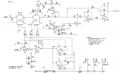
For info, recent project write-up by Tom McKay and Rod Elliott (Project 174 - Ultra-Low Distortion Sinewave Oscillator) implementing a sample and hold agc with Linsley Hood's two-stage Wien oscillator.
Project 174
I recently breadboarded the sample & hold described in this project with a view to replacing the full wave detector in an oscillator I built a while back.
The existing detector has a small amount of ripple that contributes to the harmonic distortion. Attempts to increase the time constant makes the settling time too long and can result in squegging.
The oscillator in the original project write up only operates up to 10kHz. My oscillator covers 15Hz->150kHz in 4 switched ranges.
My tests show that the S&H works up to about 28kHz.
Above that, the sampling pulses stop.
For operation at higher frequencies, C9 and C10 need to be reduced to give narrower sampling pulses.
However, this stops it working correctly at lower frequencies.
The only answer I could come up with is to switch C9 and C10 according to the frequency range.
I tried using a 4066 analogue switch to do this.
It meant reducing the +/- 12V supplies on the S&H down to +/-9v.
I was also concerned about the spikes on the input to pin 6 of the comparator.
These exceed Vcc which could damage a 4066. It needs an added protection diode between pin 6 and Vcc.
I found that using values of 1nF for C9 and 56pF for C10, the S&H can be made to operate up to about 100kHz.
Above that, the delay in the sampling pulses relative to the peak of the sinewave cause the the AGC control output to drop.
Replacing the LED 'D3' with three diodes in series helps by widening the clipped top of the sinewave. However, this reduces the AGC output voltage somewhat.
Another problem with the S&H is the unwanted offset in the AGC control output due to the FET biasing resistor R15. This is easily corrected by replacing the FET with a voltage follower using the unused half of the second TL072.
I think that's pretty impressive for a circuit with simple parts.
You can switch to a simple AGC at higher frequencies where the settling time is not an issue (Optimation did that).
Or the S/H circuit for the Boonton 1120 works to 140 KHz. One part has been discontinued from that design but ADI has newer parts that should work Sample/Track and Hold Amplifiers | Analog Devices .
The manual for the current instrument is here with details on the circuit and parts lists etc.: http://www.boonton.com/~/media/Boonton/Manuals and Software/1121A Instruction Manual.ashx
Attachments
You might be able to use 2 AD873's as a solution. Or Davida's ADC+DAC which is quite original and simple.
AD783?
- Home
- Design & Build
- Equipment & Tools
- Low-distortion Audio-range Oscillator