Photoresistor has around 15mV across it, as it is in parallel with a 15 ohm resistor. Sounds fairly low to me..
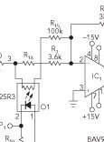
I looked at the attached part of the schematic many times since its confusing. I think the LDR is in series with the 100K resistor (limits its maximum effect and the voltage across it) and the combination is in parallel with what appears to be the 3.6K resistor and something I can't read on the schematic but I think is the 15 Ohm resistor you mentioned.
Attachments
1audio:
Yes, it is confusing. I noted in post 174 that the schematic in the article had a number of errors, among them the missing node on either side of the photoresistor. So consider the junction of the photoresistor, R18, 100k, and 3.6k to be a node. It is not shown that way in the schematic, which is in error.
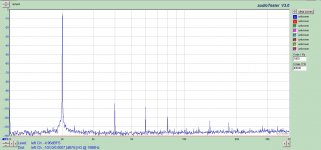
Did make some progress: the sidebands are due to distortion from too high an output level. At the time I was testing this earlier, I only checked the amplitude modulation with output level, which had no effect. Once I bring the output down to 3Vrms, I get much better results as you can see.
Annoying is the fact the amplitude modulation is still occurring, at +/- 12mV. Maybe this is the best I can expect, not sure. I have run the LED current from 6 mA (too low to control startup) to 15 mA (too high to control startup). In between works well, with 12mA settling quicker than 8mA. But each has almost identical modulation of amplitude.
I have scoped at the base of the transistor, and was able to smooth out the error signal by increasing the 100nF integrator cap to 3 uF, but this still did not resolve the output bounce (but does make it better). The 8.2K resistor right next to it does nothing, even when shorted out.
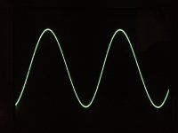
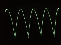
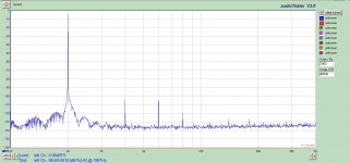
Pics also included of the sine output and output of the FW rectifier. Note the 2nd harmonic present at the output of the FW rectifier; every other valley is at alternating DC levels.
Yes, it is confusing. I noted in post 174 that the schematic in the article had a number of errors, among them the missing node on either side of the photoresistor. So consider the junction of the photoresistor, R18, 100k, and 3.6k to be a node. It is not shown that way in the schematic, which is in error.
Did make some progress: the sidebands are due to distortion from too high an output level. At the time I was testing this earlier, I only checked the amplitude modulation with output level, which had no effect. Once I bring the output down to 3Vrms, I get much better results as you can see.
Annoying is the fact the amplitude modulation is still occurring, at +/- 12mV. Maybe this is the best I can expect, not sure. I have run the LED current from 6 mA (too low to control startup) to 15 mA (too high to control startup). In between works well, with 12mA settling quicker than 8mA. But each has almost identical modulation of amplitude.
I have scoped at the base of the transistor, and was able to smooth out the error signal by increasing the 100nF integrator cap to 3 uF, but this still did not resolve the output bounce (but does make it better). The 8.2K resistor right next to it does nothing, even when shorted out.
Pics also included of the sine output and output of the FW rectifier. Note the 2nd harmonic present at the output of the FW rectifier; every other valley is at alternating DC levels.
Attachments
Nothing immediately obvious in the PCB layout. I assume you have something appropriate from the GND connection to the groundplane. I note R1 in the Wein Bridge is 54.9R rather than the schematic's 75R.
Can you tell us what the approximate frequency of the amplitude modulation is? Should be measurable or observable at TP1.
Terry
Can you tell us what the approximate frequency of the amplitude modulation is? Should be measurable or observable at TP1.
Terry
Right, there are a few differences in the PCB. I hand-matched the input RC constant to be equal to the feedback RC. If you go through the numbers from the PCB it works out. The resistor from GND to circuit common is up for experimentation once I get the output correct. Could be resistor, capacitor, jumper, or open.
Frequency of modulation is only a Hz or two. It is a little inconsistent; it holds for a bit, then bounces around and settles, then starts up again. Checked the power supplies; rock steady.
I will play around with the 15/18 ohm resistor tonight or tomorrow. It was my thinking the less effect the photoresistor has on the gain the better, but now thinking about it you may be right; higher might be better.
Good question. I figured, based on the results from the article, that all PID control issues were specifically geared for a 2 kHz frequency, so best to leave well enough alone. Otherwise, I would have geared for 1 kHz. I had received some updates from the author over email, which are incorporated in this design, hence some differences from the original schematic. Had I obtained excellent results from this design, I have 2 more PCBs, and would have attempted some other frequencies.
Yes, I can't imagine those diodes requiring extra special attention, but I do note some unevenness in the rectifier output.
Yes, I can't imagine those diodes requiring extra special attention, but I do note some unevenness in the rectifier output.
Whew, at least I'm not alone in not knowing why 2kHz!
Zigzagflux, your struggle makes this oscillator look attractive:
eBay Australia: Buy new & used fashion, electronics & home d?r
"Frequency of modulation is only a Hz or two. It is a little inconsistent; it holds for a bit, then bounces around and settles, then starts up again. Checked the power supplies; rock steady."
This seems to suggest it's not a straightforward loop instability issue - you would expect that to be cyclical. I'd also check the stability of the reference voltage.
Might be worth checking any connections or components you have any reason to have doubts about.
The approach has a lot in common to one of the references at the end of the article:
http://cds.linear.com/docs/Article/ubm_edn_20110811 18Bit ADCs Ad Free.pdf
(Also 2kHz, hmmmmm....) Perhaps worth contemplating the differences?
Terry
Whew, at least I'm not alone in not knowing why 2kHz!
Zigzagflux, your struggle makes this oscillator look attractive:
eBay Australia: Buy new & used fashion, electronics & home d?r
Terry
Has anyone actually bought one of these and tested it out?
There a lot of talk about them but I haven't heard of any reports.
David.
Annoying is the fact the amplitude modulation is still occurring, at +/- 12 mV. Maybe this is the best I can expect, not sure.
To check the stability of the level control loop I suggest to modulate the reference voltage with a low-frequency (perhaps 10 Hz, or even 1 Hz) square wave. The response observed at the oscillator output or at the integrator output should be reasonably well-damped. If not, try setting the integrator zero at lower frequency.
Can you post the exact schematic you're using?
Samuel
Hi,
I tried simulating the circuit and it seems it is really very picky in the AGC behaviour. The LDR coupler was modelled with a controlled resistor, running along an 1/Iset curve around 80Ohms @ 10mA which matched the published number and graphs quite well (but not the response time). I used a Zener to clamp the top integrator output because of ideal opamps used. Startup is triggered by injecting one single period of the osc. freq. at the beginning. Find LTspice simulation file attached (rename to .asc).
The noted asymetric behaviour of the rectifier is confirmed in the sim, too (depends on the diode load resistor and the comp cap).
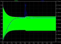
I finally managed to get to a stable operating point, playing with the series and parallel resistor around the LDR.
Injecting a step at the AGC reference, as per Samuels suggestion, shows a quite well damped response. See screenshot.
But whenever missing the correct parameter range even by a slight amount the osc either died or showed some sort of "gain hiccuping" with 1s order of magnitude period times, just what ZigZag is seeing.
I would think the circuit is very sensitive and might easily be working "just on the edge" where small amounts of noise and other disturbances or drifts could upset stability.
I'd like to see the outcome of this and even try it myself, the game is : will it beat my trusty Tek SG505 (which I think is a masterpiece of an adjustable osc)?
I tried simulating the circuit and it seems it is really very picky in the AGC behaviour. The LDR coupler was modelled with a controlled resistor, running along an 1/Iset curve around 80Ohms @ 10mA which matched the published number and graphs quite well (but not the response time). I used a Zener to clamp the top integrator output because of ideal opamps used. Startup is triggered by injecting one single period of the osc. freq. at the beginning. Find LTspice simulation file attached (rename to .asc).
The noted asymetric behaviour of the rectifier is confirmed in the sim, too (depends on the diode load resistor and the comp cap).
I finally managed to get to a stable operating point, playing with the series and parallel resistor around the LDR.
Injecting a step at the AGC reference, as per Samuels suggestion, shows a quite well damped response. See screenshot.
But whenever missing the correct parameter range even by a slight amount the osc either died or showed some sort of "gain hiccuping" with 1s order of magnitude period times, just what ZigZag is seeing.
I would think the circuit is very sensitive and might easily be working "just on the edge" where small amounts of noise and other disturbances or drifts could upset stability.
I'd like to see the outcome of this and even try it myself, the game is : will it beat my trusty Tek SG505 (which I think is a masterpiece of an adjustable osc)?
Attachments
The PCB layout looks OK.
It might be possible to clean up the full wave rectifier output a little.
I have built some full wave rectifiers myself a long time ago and found that 'Applications of Operational Amplifiers' by Jerald G. Graeme helpful. I think that the alternating DC values are due to the offset voltage of the first operational amplifier stage TL082D. The switching around 0 V is also affected by the slew rate and high frequency small signal gain of the TL082. So a lower offset, higher bandwidth, greater slew rate operaational amplifier should help. It might also be worth using schottky diodes for their lower forward voltage but with the disadvantage of higher capacitance and leakage.
I agree with KSTR the circuit amplitude will be working on an edge. It's got two frequency roll off stages in series in the control loop with the integrator and the filter on the transistor base along with the delay in amplitude change in the Wien bridge.
After studying the ebay pcb pix, I thought it appeared similar to a JanasCard inverting Wien bridge but with a jfet AGC. The seller said it was similar but used his own AGC jfet design with 1/2 D-S fed to G for second harmonic reduction.Whew, at least I'm not alone in not knowing why 2kHz!
Zigzagflux, your struggle makes this oscillator look attractive:
eBay Australia: Buy new & used fashion, electronics & home d?r
The seller also indicated he was comtemplating posting the schematic here or on his ebay ad.
A couple of these with a good summer and output circuit could make a nice IM generator.
Just seems like the AGC control range is too small. I'd try making the 18R resistor larger, say 27R. I think I'd make the 10uF at the base of the transistor larger too.
Good call. Increased R18 from 15 to 22, to 47, and finally 63. Improvement each time with gain control. Now getting about +/- 0.5mV of wobble, and its pretty consistent and doesn't get out of control. Also notice that stability is best when the current through the LED is low, around 4-5 mA. May not be best for linearity, as I can see my 3rd harmonic is a little higher, but we are stable. Starts up and settles very quickly, too.
The cap at transistor base was about the same when increased by 10uF, but got unstable with an extra 22uF.
At this point I have determined that my simple D/A through transformer works better. If (and that's a big if) the author really did get distortion measurements that low, the design is way too marginal and sensitive to luck that it's not worth pursuing anymore.
I will keep watch over the test results from the ebay oscillator. It was worth a try. Thanks for the help.
Attachments
@zigzag -- You're not seeing the real performance of the oscillator, just the residual of your ADC. I suggest you build a pre-filter, hopefully an active twin-tee notch filter to reduce the fundamental level while leaving the harmonics unattenuated. This will reveal the harmonics accurately. For one way, see my page Active Twin-T notch filter.
- Home
- Design & Build
- Equipment & Tools
- Low-distortion Audio-range Oscillator