
Hello,
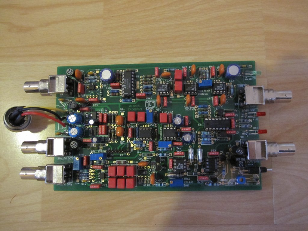
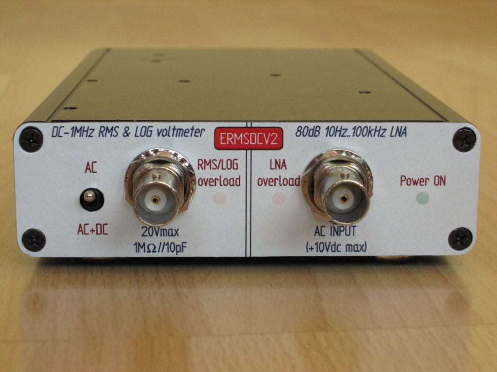
The Hammond enclosure is fully drilled and the board fit very well.
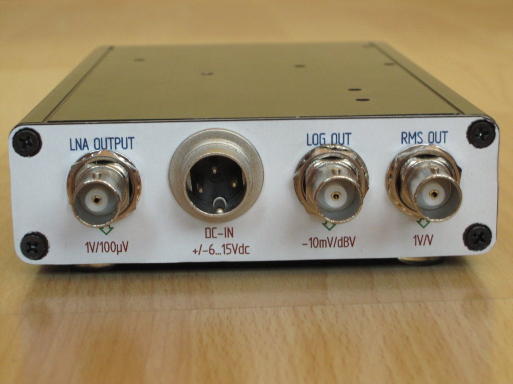
I have also designed a laser printable sticker as a silkscreen for front and rear panel. It's easy to do and result is pretty good.
I will add it in the next design folder of this project that i prepare.
You can see the result on pictures below.
Next step now, is to test it !")
I'll do that this saturday. To soon.
Frex.
The Hammond enclosure is fully drilled and the board fit very well.
I have also designed a laser printable sticker as a silkscreen for front and rear panel. It's easy to do and result is pretty good.
I will add it in the next design folder of this project that i prepare.
You can see the result on pictures below.
Next step now, is to test it !
I'll do that this saturday. To soon.
Frex.
ERMSDCV2-- All measurments results.
Hello,
After soldering all parts, do the functional tests and drill it's enclosure,
i have run many measurements on my ERMSDCV2 to qualify it's practical specs.
Test concern the three functions of the ERMSDCV2 design :
_The DC..1MHz RMS to DC converter
_The LOG AC voltmeter.
_The 80dB 10Hz..100kHz LNA
As you will see below, results are very good. The instruments could be really
useful for audio/electronics investigations.
I have write a test and trimming procedure allowing very simple adjustment
to get a fully functional and calibrated device. I will send new documents to all PCB buyers.
Note that i had need to do some little modifications on the design to correct mistakes.
(Please read the wiki main page about that). This will be also included in new files.
You can download the latest schematic version (including all modifications)
here : ERMSDCV2.3_sch.pdf .
Otherwise specified, all tests are made using 1X probe (a coaxial cable) with the
jumper W3 closed, and front panel switch in DC position (down).
The device is powered by a +/-9VDC linear PSU.(+/-6v to +/-15v maxi)
1/ The DC..1MHz RMS to DC converter.
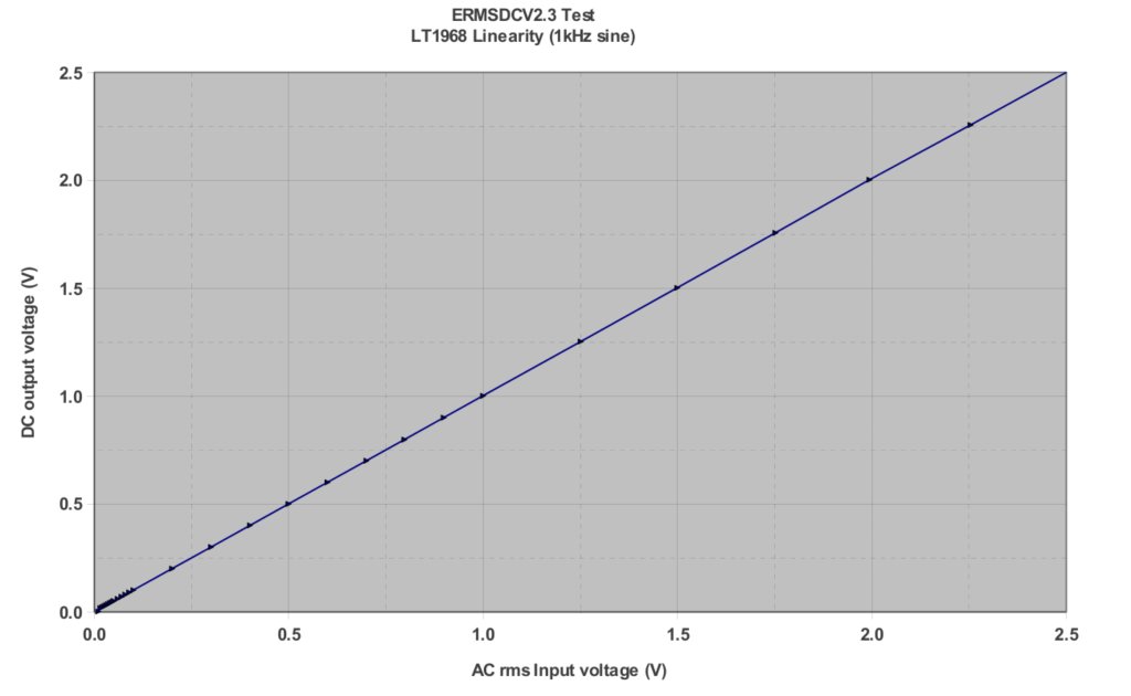
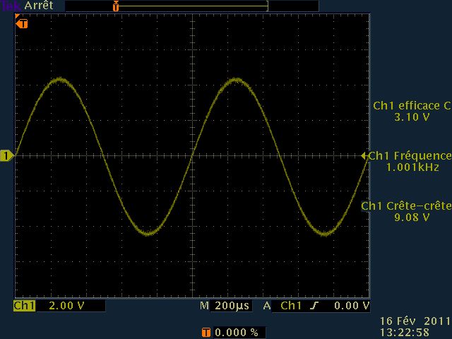
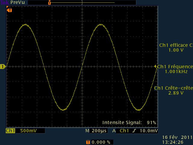
1.A/ Linearity test.(DC output level vs AC input level for 1kHz sine wave).
As you see, the RMS converter work very good from about tenth mV to more than 2.5V.
The usable lower limit is about 20mV (<10% error).
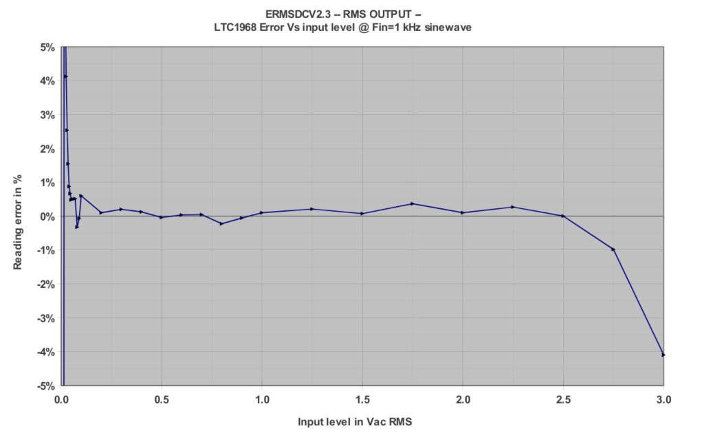
1.B/ Measurement error test.(Error in % of input level for 1kHz sine wave).
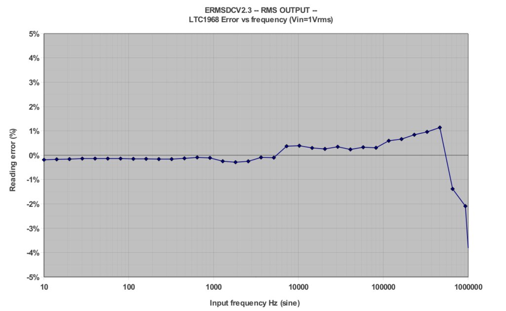
1.C/ Frequency response measurement test.(Error in % of input vs frequency for 1Vrms sine wave).
The error versus frequency show very good linearity up to 400kHz and fall at about 600kHz.
The frequency flatness depend largely on the AD817 low-pass filter Butterworth conformance (set to 1.8MHz cutoff).
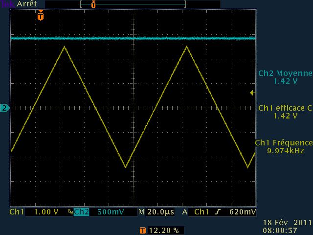
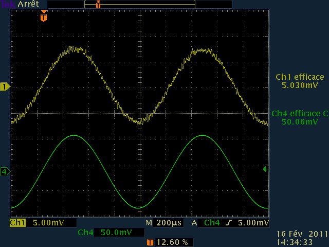
1.D/ 5Vpk-pk 10kHz Triangular wave RMS measurement test. (Yellow=signal input , Blue trace= DC output).
Here i test the RMS conversion of triangular wave (crest factor of 1.7).
1.E/ 2.5Vpk-pk 5% duty-cycle rectangular wave RMS measurement test. (Yellow=signal input , Blue trace= DC output).
Test with high crest factor signal (here 4.5), the RMS conversion stay very good despite this.
1.F/ Digital pink noise RMS measurement test. (Yellow=signal input , Blue trace= DC output).
Test with random digital pink noise, again very good RMS conversion.
I have also try measurements with x10 and x100 scope probe (W3 jumper open),
allowing the extend of measurement range, and it work fine.
You just need to trim your probe compensation for frequency flatness and then you can measure up to 300Vrms!
(with a 100x probe)
2/ The LOG AC voltmeter.
Note: To test the log voltmeter output, the input signal must be very very low,
so i use precision shielded passive voltage divider to get the right input level.
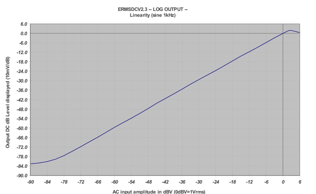
2.A/ Linearity test.(DC output level normalized as dB vs AC input level for 1kHz sine wave).
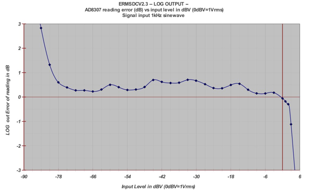
2.B/ Measurement error test.(Error in dB of input level for 1kHz sine wave).
2.C/ Log output frequency response test.(Vin=1Vrms).
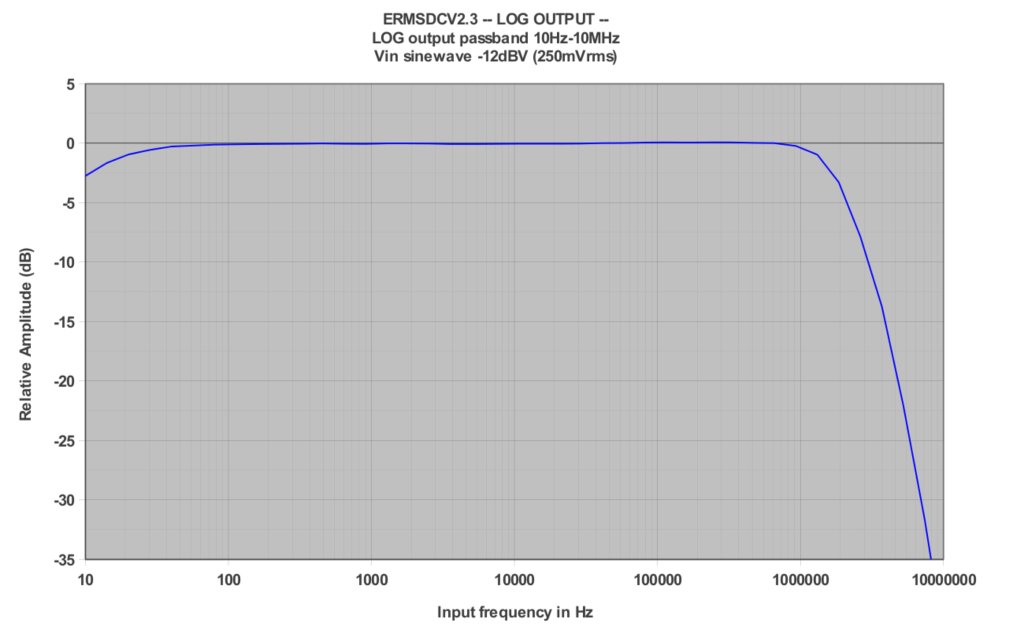
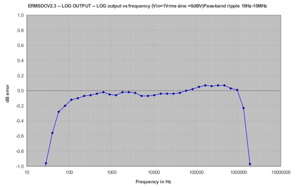
2.D/ Log output frequency response test, zoomed view of the previous graph.(Vin=1Vrms).
The front-end of the LOG voltmeter(U16-U12)) use an OPA627 followed by an AD817.
The noise floor of the log voltmeter depend largely of the noise of these two IC.
On my design, with 0dBV calibrated to 1Vrms, i get a noise floor of about
-84.5dBV 60µV).The AD8307 noise floor is about -90dBV.
As you see the frequency flatness is about +/-0.1dB in 100Hz-1MHz range !
3/ The 80dB 10Hz..100kHz Low Noise Amplifier.
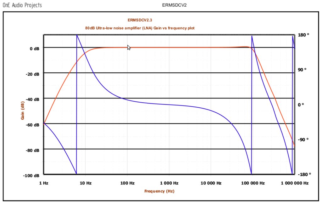
3.A/ LNA frequency response test (normalized).(Vin=100µVrms red= Gain , blue=Phase).
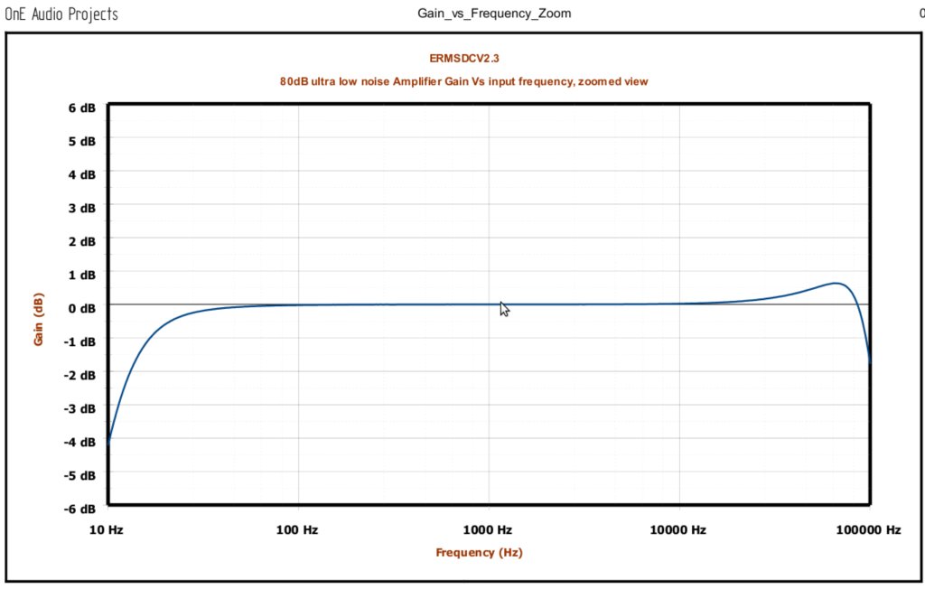
3.B/ LNA frequency response test, zoomed view (normalized).(Vin=100µVrms red= Gain , blue=Phase).
3.C/ LNA maximum output voltage before saturate.(Vin=310µVrms Yellow=LNA output).
3.D/ LNA output voltage for 100µV 1kHz sinewave input.(Vin=310µVrms Yellow=LNA output).
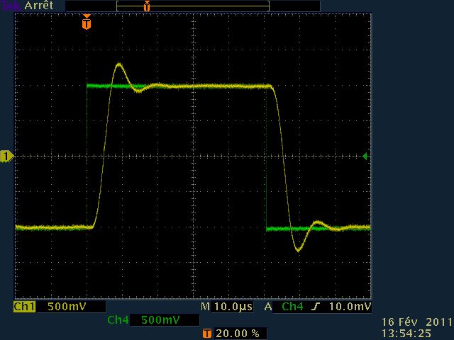
3.E/ LNA pulse response.(Vin=+/-100µV 10kHz square wave Green=signal input before attenuator Yellow=LNA output).
This test show clean response of the Butterworth fifth order low pass filter.
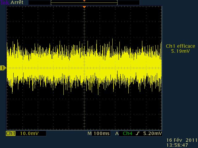
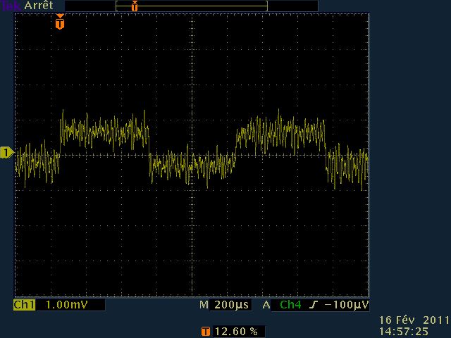
3.F/ LNA noise floor.(No signal, 50 Ohms plug on LNA input, Yellow=LNA output).
This signal show the own output noise of the LNA.This represent about 520nV RTI (Referred To Input).
It's mainly the noise of input OPAMPs, this is why they must have very good noise specs.
3.G/ LNA low level signal reconstruction.(Vin=500nV 1kHz sinewave Green=signal input before attenuator
Yellow=LNA output).
Using the scope digital averaging to eliminate the uncorrelated noise, you can show clearly a sinwave signal
as small as 500nVrms.
The 50mV (green trace) is attenuated by 100dB (1/100000) before to go at LNA input.
3.H/ LNA Ultra low level signal reconstruction.(Vin=100nV 1kHz square wave Yellow=LNA output).
Here, it's same as previous screenshot, with 100nV pk-pk square wave signal and scope digital averaging.
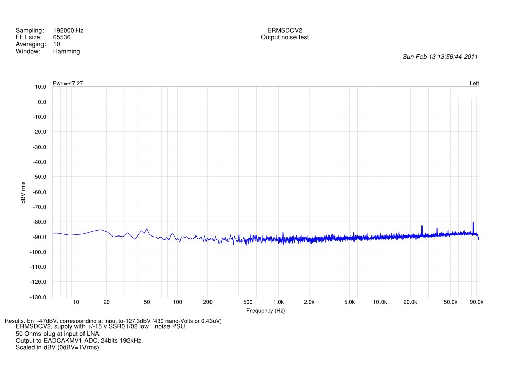
3.F/ LNA noise floor spectral view. (No signal, 50 Ohms plug on LNA input, Blue=LNA output spectrum).
Here, the full output spectrum of the LNA output noise.The noise is very flat in all bandwidth, showing white noise type.
No visible harmonics of main (50/60Hz and multiples) and no spurious.
The ADC show a RMS level of -47.27dBV that correspond to about 4.33mVrms. (433nV RTI)
Roughly the same measurement value done with scope on section 3.F.
-----------------
Ouf ! I'm sorry this long reading...But if it's any consolation, it was even longer for me to write that ! ;-)
I hope all builders will be happy with their devices. For me, that will be a new useful "DIY" instrument in my lab.
Don't hesitate if you have any question, i will always try to answer you.
Regards.
Frex.
Many others info and files for download can be find on the dedicated wiki page HERE . Thank's !
(Note that i still have some PCB available for this design, i you're interested just send me a PM).
Hello,
After soldering all parts, do the functional tests and drill it's enclosure,
i have run many measurements on my ERMSDCV2 to qualify it's practical specs.
Test concern the three functions of the ERMSDCV2 design :
_The DC..1MHz RMS to DC converter
_The LOG AC voltmeter.
_The 80dB 10Hz..100kHz LNA
As you will see below, results are very good. The instruments could be really
useful for audio/electronics investigations.
I have write a test and trimming procedure allowing very simple adjustment
to get a fully functional and calibrated device. I will send new documents to all PCB buyers.
Note that i had need to do some little modifications on the design to correct mistakes.
(Please read the wiki main page about that). This will be also included in new files.
You can download the latest schematic version (including all modifications)
here : ERMSDCV2.3_sch.pdf .
Otherwise specified, all tests are made using 1X probe (a coaxial cable) with the
jumper W3 closed, and front panel switch in DC position (down).
The device is powered by a +/-9VDC linear PSU.(+/-6v to +/-15v maxi)
1/ The DC..1MHz RMS to DC converter.
1.A/ Linearity test.(DC output level vs AC input level for 1kHz sine wave).
As you see, the RMS converter work very good from about tenth mV to more than 2.5V.
The usable lower limit is about 20mV (<10% error).
1.B/ Measurement error test.(Error in % of input level for 1kHz sine wave).
1.C/ Frequency response measurement test.(Error in % of input vs frequency for 1Vrms sine wave).
The error versus frequency show very good linearity up to 400kHz and fall at about 600kHz.
The frequency flatness depend largely on the AD817 low-pass filter Butterworth conformance (set to 1.8MHz cutoff).
1.D/ 5Vpk-pk 10kHz Triangular wave RMS measurement test. (Yellow=signal input , Blue trace= DC output).
Here i test the RMS conversion of triangular wave (crest factor of 1.7).
1.E/ 2.5Vpk-pk 5% duty-cycle rectangular wave RMS measurement test. (Yellow=signal input , Blue trace= DC output).
Test with high crest factor signal (here 4.5), the RMS conversion stay very good despite this.
1.F/ Digital pink noise RMS measurement test. (Yellow=signal input , Blue trace= DC output).
Test with random digital pink noise, again very good RMS conversion.
I have also try measurements with x10 and x100 scope probe (W3 jumper open),
allowing the extend of measurement range, and it work fine.
You just need to trim your probe compensation for frequency flatness and then you can measure up to 300Vrms!
(with a 100x probe)
2/ The LOG AC voltmeter.
Note: To test the log voltmeter output, the input signal must be very very low,
so i use precision shielded passive voltage divider to get the right input level.
2.A/ Linearity test.(DC output level normalized as dB vs AC input level for 1kHz sine wave).
2.B/ Measurement error test.(Error in dB of input level for 1kHz sine wave).
2.C/ Log output frequency response test.(Vin=1Vrms).
2.D/ Log output frequency response test, zoomed view of the previous graph.(Vin=1Vrms).
The front-end of the LOG voltmeter(U16-U12)) use an OPA627 followed by an AD817.
The noise floor of the log voltmeter depend largely of the noise of these two IC.
On my design, with 0dBV calibrated to 1Vrms, i get a noise floor of about
-84.5dBV 60µV).The AD8307 noise floor is about -90dBV.
As you see the frequency flatness is about +/-0.1dB in 100Hz-1MHz range !
3/ The 80dB 10Hz..100kHz Low Noise Amplifier.
3.A/ LNA frequency response test (normalized).(Vin=100µVrms red= Gain , blue=Phase).
3.B/ LNA frequency response test, zoomed view (normalized).(Vin=100µVrms red= Gain , blue=Phase).
3.C/ LNA maximum output voltage before saturate.(Vin=310µVrms Yellow=LNA output).
3.D/ LNA output voltage for 100µV 1kHz sinewave input.(Vin=310µVrms Yellow=LNA output).
3.E/ LNA pulse response.(Vin=+/-100µV 10kHz square wave Green=signal input before attenuator Yellow=LNA output).
This test show clean response of the Butterworth fifth order low pass filter.
3.F/ LNA noise floor.(No signal, 50 Ohms plug on LNA input, Yellow=LNA output).
This signal show the own output noise of the LNA.This represent about 520nV RTI (Referred To Input).
It's mainly the noise of input OPAMPs, this is why they must have very good noise specs.
3.G/ LNA low level signal reconstruction.(Vin=500nV 1kHz sinewave Green=signal input before attenuator
Yellow=LNA output).
Using the scope digital averaging to eliminate the uncorrelated noise, you can show clearly a sinwave signal
as small as 500nVrms.
The 50mV (green trace) is attenuated by 100dB (1/100000) before to go at LNA input.
3.H/ LNA Ultra low level signal reconstruction.(Vin=100nV 1kHz square wave Yellow=LNA output).
Here, it's same as previous screenshot, with 100nV pk-pk square wave signal and scope digital averaging.
3.F/ LNA noise floor spectral view. (No signal, 50 Ohms plug on LNA input, Blue=LNA output spectrum).
Here, the full output spectrum of the LNA output noise.The noise is very flat in all bandwidth, showing white noise type.
No visible harmonics of main (50/60Hz and multiples) and no spurious.
The ADC show a RMS level of -47.27dBV that correspond to about 4.33mVrms. (433nV RTI)
Roughly the same measurement value done with scope on section 3.F.
-----------------
Ouf ! I'm sorry this long reading...But if it's any consolation, it was even longer for me to write that ! ;-)
I hope all builders will be happy with their devices. For me, that will be a new useful "DIY" instrument in my lab.
Don't hesitate if you have any question, i will always try to answer you.
Regards.
Frex.
Many others info and files for download can be find on the dedicated wiki page HERE . Thank's !
(Note that i still have some PCB available for this design, i you're interested just send me a PM).
Hello Frex,
The results are very impressive, including your very extensive and professional testing. So first of all many thanks for making this happen. The questions that I have right now are:
1. The LTC1968 is really tiny. How did you manage to solder it to the PC board - are there any special tricks? I had already ordered a sample (and of 1967) a long time ago but did not venture using them until your project came along.
2. The OPA627 is very expensive, what I saw so far is well above EUR 20,--. Are there any equivalent OpAmps with the same specs that we might substitute? I can go and file through spec sheets but maybe you know some already.
The results are very impressive, including your very extensive and professional testing. So first of all many thanks for making this happen. The questions that I have right now are:
1. The LTC1968 is really tiny. How did you manage to solder it to the PC board - are there any special tricks? I had already ordered a sample (and of 1967) a long time ago but did not venture using them until your project came along.
2. The OPA627 is very expensive, what I saw so far is well above EUR 20,--.
Are there any equivalent OpAmps with the same specs that we might substitute? I can go and file through spec sheets but maybe you know some already.Hello,
MRupp,
i soldered the LT1968 (MSOP package) using a small iron tip, a good light and a magnifying glass. Of this work require very good eyes !
You can also to try a method that consisting in place the IC, and then doing a big solder along each sides and remove excess of tin with a desoldering braid.
You can find many video showing how to do that, on Youtube for example.
You can replace the OPA627 OPAMP by others, with FET input(low Ibias), high frequency bandwidth and low noise. The AD711 can be good low cost choice. Many others can work too. Note that if you need to use the LOG output, the measurements noise floor depend on this IC (and the AD817).
Andrew T,
I'm sorry but i don't want to organize that, it will take a time that i don't have.
But of course, you can do it !
Regards.
Frex
Hello,
I'm a little surprised about the little readers comments.
I have made today new measurements that i don't have done before.
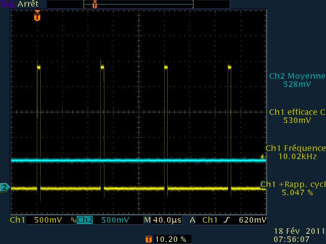
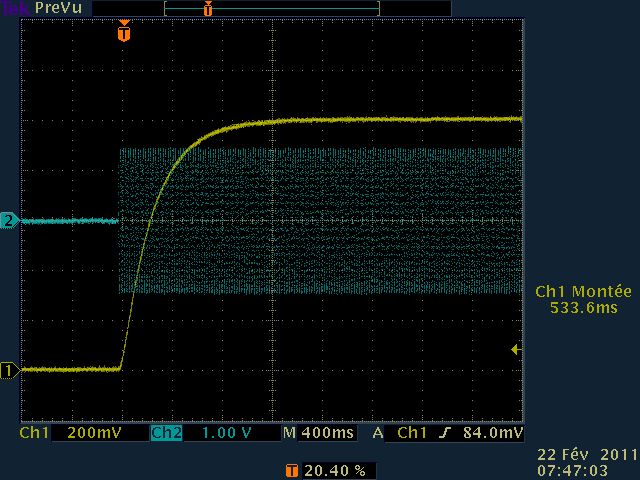
RMS to DC converter settling time.
The input signal is a 1Vrms 100Hz sine-wave (blue), the output in yellow
show the response time.
As you could see on the picture, the output settle in about 500ms.
(front panel switch in DC mode).
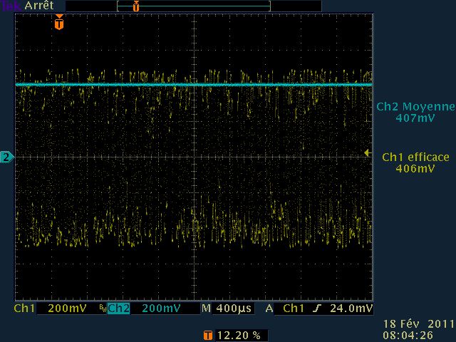
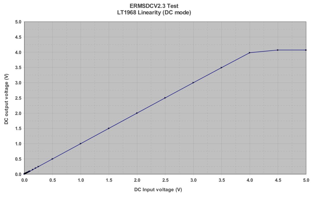
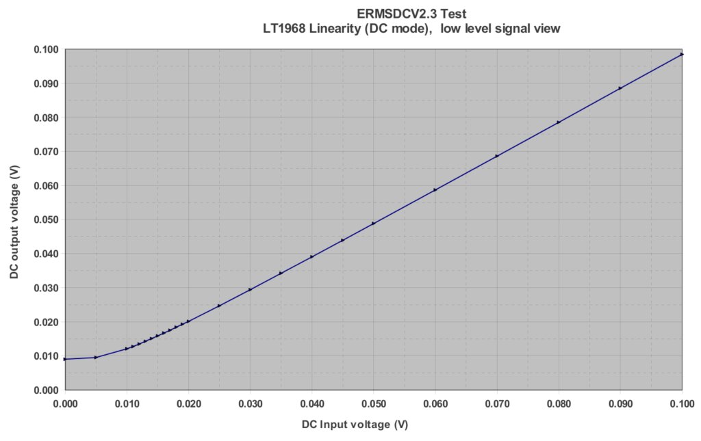
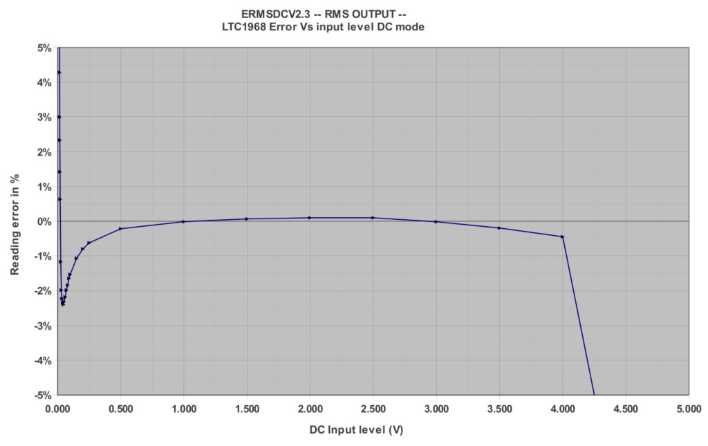
RMS to DC converter DC linearity .
In these tests i use a DC scignal to be measured by the ERMDCV2.
(front panel switch in DC mode).
A/ Linearity vs DC input level 0 to 5VDC .
B/ Linearity vs DC input level zoomed view, 0 to 250mVDC.
C/ % Error vs DC input level 0 to 5VDC .
C/ % Error vs DC input level 0 to 250mVDC .
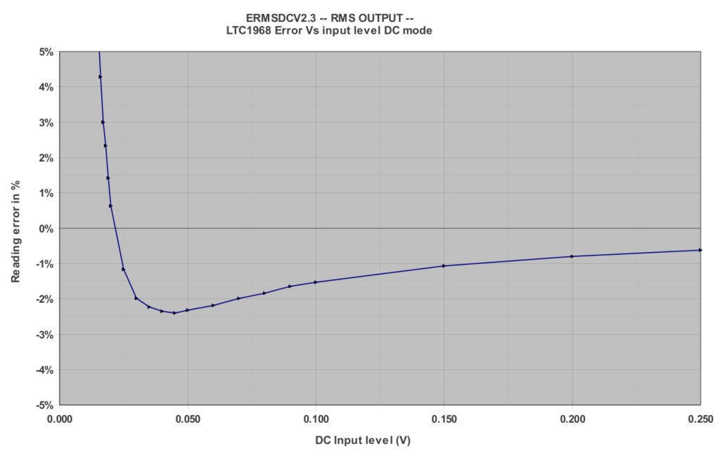
Note that all measurements i have done has been made with precision calibrated DC voltmeter and DC generator.
To summarize, i'm very happy about all results obtain.
The LTC1968 and the AD8307 really keep their promise and offer very good solution.
My next DIY project that i will post, will change a little of previous.
I design a small laboratory SMPS based on resonant fly-back converter.
It's specs will be ; 75w output power, 2 symmetric variable outputs (+/-5..+/-15V) and another output of +3 to +9V.Each output could handle 2Amp, small standard Hammond enclosure, low output noise, easy to build.
Of course, i will do new post when i will be ready.
(The project have already seriously progressed)
Frex.
I'm a little surprised about the little readers comments.
I have made today new measurements that i don't have done before.
RMS to DC converter settling time.
The input signal is a 1Vrms 100Hz sine-wave (blue), the output in yellow
show the response time.
As you could see on the picture, the output settle in about 500ms.
(front panel switch in DC mode).
RMS to DC converter DC linearity .
In these tests i use a DC scignal to be measured by the ERMDCV2.
(front panel switch in DC mode).
A/ Linearity vs DC input level 0 to 5VDC .
B/ Linearity vs DC input level zoomed view, 0 to 250mVDC.
C/ % Error vs DC input level 0 to 5VDC .
C/ % Error vs DC input level 0 to 250mVDC .
Note that all measurements i have done has been made with precision calibrated DC voltmeter and DC generator.
To summarize, i'm very happy about all results obtain.
The LTC1968 and the AD8307 really keep their promise and offer very good solution.
My next DIY project that i will post, will change a little of previous.
I design a small laboratory SMPS based on resonant fly-back converter.
It's specs will be ; 75w output power, 2 symmetric variable outputs (+/-5..+/-15V) and another output of +3 to +9V.Each output could handle 2Amp, small standard Hammond enclosure, low output noise, easy to build.
Of course, i will do new post when i will be ready.
(The project have already seriously progressed)
Frex.
would it be worth doing a group buy of the "kit" components?
Best thing to do in a case like this is to use the "Bill of Materials Tool" at one of the US Distributors -- DK probably best here as they carry Linear Tech (Mouser doesn't). Pete Millett offered a BOM via an Excel spreadsheet for the "Engineers Amplifier" -- you could just download it to Mouser's site. (Don't know if Pete is fond of Mouser, but, of course, both are in Texas!)
ERMSDCV2 new files.
Hello,
I've doing many work on the project and i posted some new documents:
_ A user manual to understand and doing measurements.
_ A full measurements report do with my ERMSDCV2.
These documents can be downloaded below,
Note that some bare PCB are available for sale (25€each, worldwide shipping included ). If you're interested, just send me a PM.
Frex.

Frex,
I'm interested in the gain block part of your device. As I compare your schematic to AN83, I have a couple of questions;
1. why did you subsitute the AD859 (U10) for the LT1224 (A3)
2. You put an additional gain block after the LTC1562, is this important, or just to jump the voltage another 10x?
Thanks,
Ken
Hello Ken,
The answers are ;
1/ The AD8597 replace the LT1028 (not LT1224) as low noise input stage,
because the it cost much less for quite similar performance. Of course you can use both
in my PCB design because it allow SOIC8 or DIP8 parts.
2/ Yes i've add a last 20dB gain block after the LTC1562 to get more sensitive output.
This stage is not very critical in term of noise and bandwidth. The advantage of OP162 is to be rail-to-rail output so get the maximum dynamic range.
I hope that help you.
Regards.
Frex
Hello Frex,Hello,
As some DIYers have already seen, i love to build measurements tools.
I have build some times ago a very useful tool, based on the AN83 and AN61 from a Linear Technology.
It's a wideband DC..10MHz RMS to DC converter (AN61) and a very low noise, high-gain, 10Hz-100kHz filtered amplifier(AN83).
This two tools together (or not) are intended to be used for electronics noise maesurements.
I had build it to compare noise produced by differents voltage regulators.
For a this use, the two functions are connected one behind the other, and a DC voltmeter is connected at the output of RMS/DC converter to
display directly the noise level measurement at input of the LNA.
This two function are indépendant but located on the same enclosure.
These tools works fine.So the RMS/DC converter described in the AN61 use an obsolete part, the LT1088.
This part is hard to find, and if you find one you risk to get it at very high cost !
Another issue with this part is it's unabality to doing measurements when signal level is too low.
So, it's practical measurement range is limited to about 10 to 100% of full scale.
On the other hand, the major advantage of this circuit is to allowing measurement at frequency up to 50MHz,
with signal with crest factor very high without degrading the precision.
You can see what does look this first version below.It's a self made PCB.
[Pict1]
Some weeks ago i had decided to make a new version of this tool.
I want to replace the LT1088 with a modern solution and an easy to find part, to make it more buildable.
Then i think it would be an interesting projects to many DIYers...Isn't it ?
Not many solutions exist to doing RMS-DC conversion, above at reasonable cost.
I eliminate the very known log-antilog converter (like AD736) because they are cosly, doesn't have
wide bandwidth, have big error with crest factor increase.
Nowadays, a good solution is to use a new IC from Linear Tech, the LTC1968 (again they !)
This relatively new IC use an innovative way to do RMS-DC convertion.
It allow very good bandwidth of up to 1MHz, very good precision of less than 1% and low cost.
The measurement precision stay very good with low signal level and medium crest factor.
The LTC1968 is also very easy to do work, only few parts are need to be fully fonctionnal.
The only issue is that it only exist in a very tiny SMD package (MSOP8), to require a good soldering tip.
So, unfortunatly for humans eyes it's quite often the case with modern electronics parts....
The main specifications i would ask for each functions of the new measurement tool are :
Common specifications:
* Powered by batteries (+/-6Vdc) or symetric DC supply +/-6V to +/-12V.
* Housed in low cost aluminium case Hammond 1455L1601.
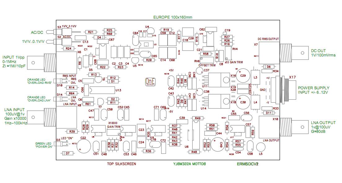
* Standard Europe 100x160mm 2 layers PCB.
* No exotic parts.
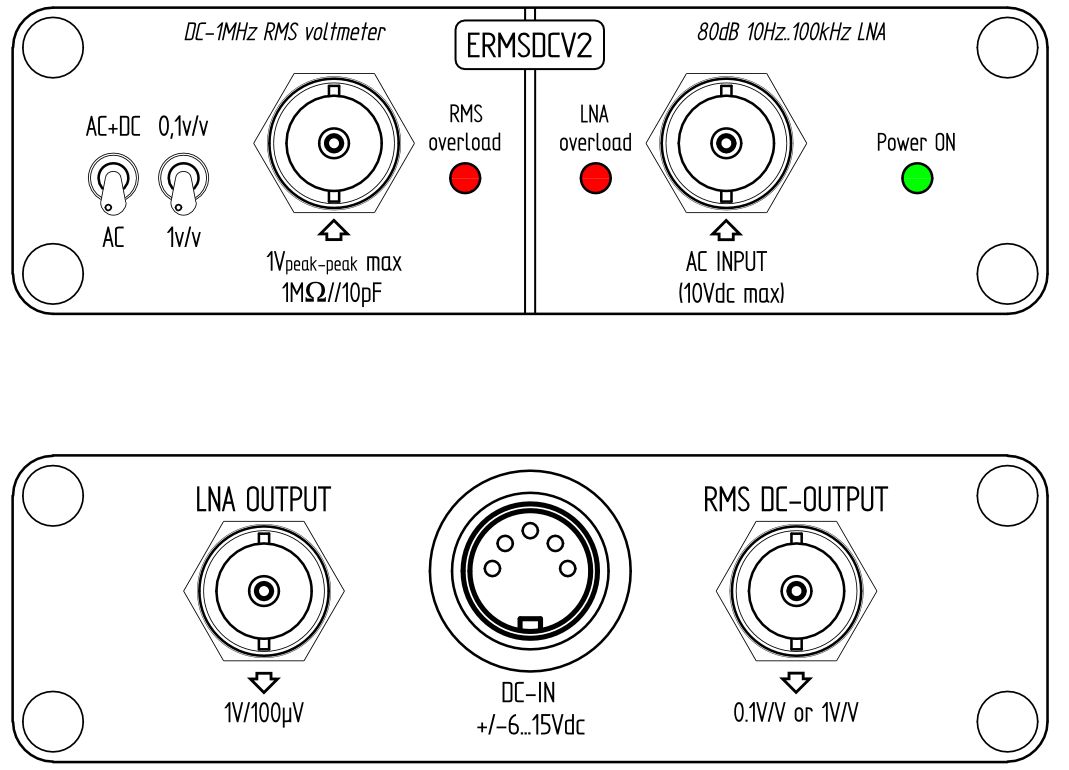
1/ Low Noise Amplifier (LNA):
* High gain of 80dB (x 10 000)
* 10Hz..100kHz build-in -3dB pass-band filter.
* Equivalent input noise of about 500nVrms.
* BNC input and output.
* Overload detection.
1/ RMS to DC converter:
* DC to 1MHz measurement bandwidth
* High input impedance 1MOhms/10pF
* Ooscilloscope probe use for x10/x100 attenuation,
allowing extending measurement range.
* 1v/100mV or 1V/V sensitivity output.
* BNC output and output.
* Overload detection.
* AC or DC coupling input.
You can see below the functionnal synoptic of the new projects ERMSDCV2 with above features :
[Pict2]
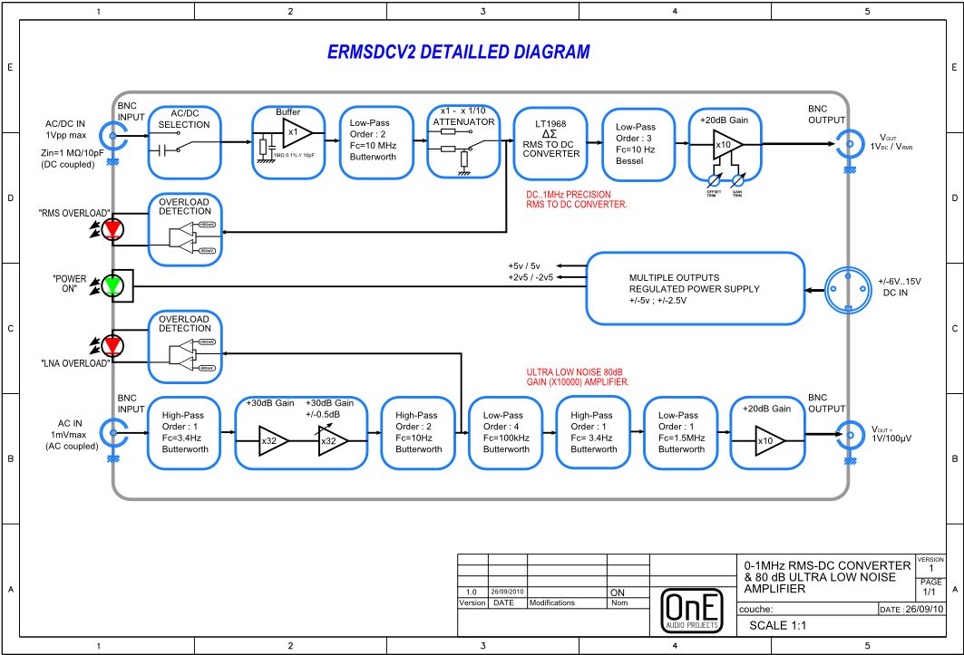
The LNA doesn't change in the V2, just an overload detection is added, and the possibility to use SMD or DIP parts(dual-pattern).
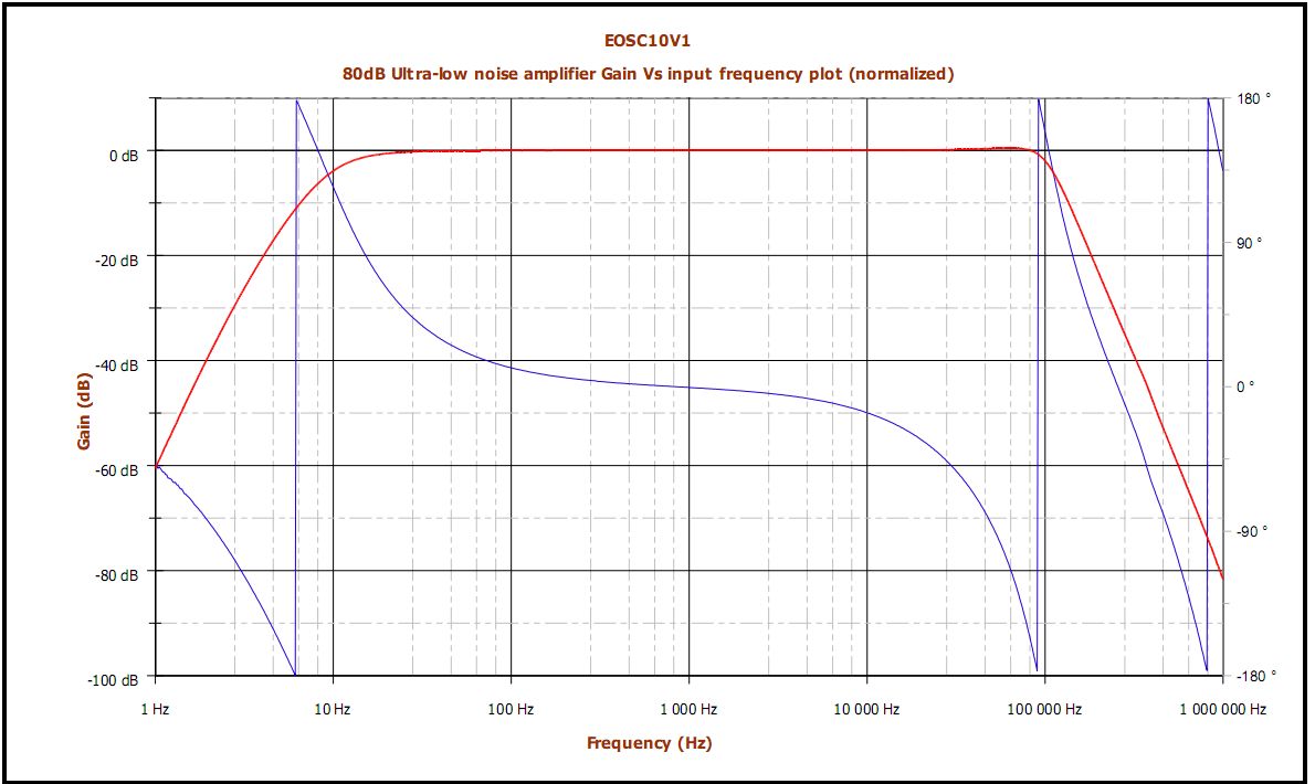
You can see below the resulting frequency response of the LNA, and it's own output spectrum with shorted input.
(It's not simulation results, but real measurements !)
[Pict3]
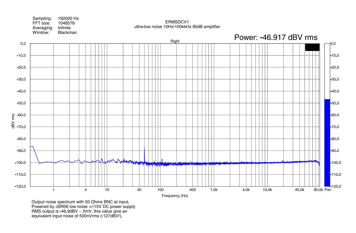
[Pict4]
As you see, the measured output noise level of the LNA is about 5mVrms (-47dBV), so it's about 450nVrms reffered to the input (-127dBV)!
(It's the equivalent noise generated by a 150 Ohms resistor at 300°K !)
This very low noise level in this frequency band allow to do measurements in microvolt range. Like regulators noise, amplifiers noise and more.
To achieve this specs, shielding is very important ! An very good power supply or using batteries is recommanded for measuring this level of noise.
50/60Hz line magnetic field can be an issue, so all transformers must be far to the setup measurement, if possible.
The new schematic of the ERMSDCv2 is done, you can download it HERE (pdf file).
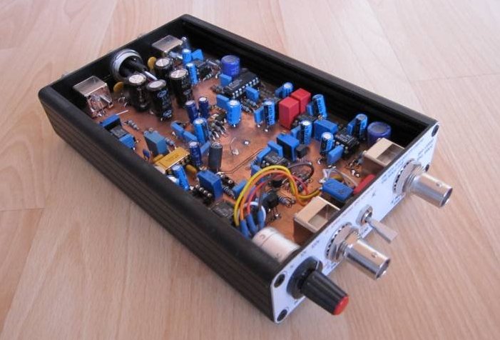
The final design in it's hammong box will look like this ;
[Pict5]
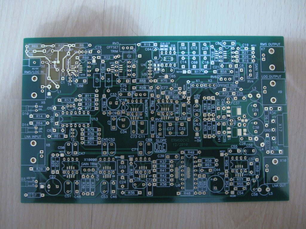
And the printed circuit boards will look like this ;
[Pict6]
Actually i start to solder parts on the prototype PCB and wait to receive some missing parts.
Of course, i will post results as soon i will try it.
I hope that new projects will interest many electronics fanatic like me. ;-).
As for the "AN67 10kHz low THD oscillator" and "DIY CS5381 ADC" ,
when the project will be ok i will organize a PCB group-buy for this new design
if some DIYers are interested.
To follow soon...
Frex.
accidentally I've found your project in the www while looking for results regarding the LTC1088
This board seemed to be made with the EAGLE board-layout, right?
If yes, would you like to send over the CAD-file for board production,
because I would like to send it to a german pcb manufacturer who do the
board production in good quality at reasonable price for me, and,
how much do I have to pay you for the CAD-file?
Kind regards from Germany to France,
Michael
Hello Michael,
The ERMSDCV2 has been made using PCAD software (become now Altium).
I have sold many PCB of this design to DIYaudio members, and at this time i still have a few available for sale if you want build one.
(I ask 30€ for one board including worldwide shipping and a very complete design
folder send by e-mail).
Note that the ERMSDCV2 use the LTC1968 IC for RMS conversion instead of my first version (ERMSDCV1) that use the older, expensive and very hard find LT1088.
If you want know more about the design, you can read the manual, and the
full measurements report.
Regards.
Frex
More
- Home
- Design & Build
- Equipment & Tools
- New DIY Project for measuring noise : 10Hz..100kHz LNA // 1MHz RMS-DC converter