Why wouldn't you place a separate current setting resistor for each pair?At a given Vgs some carry 150 mA while others still are completely closed.
C2 will pick all possible interferenceThere is no feedback. Must sound ooooh, so goood!
The bottom line is that little of the theory led to solutions, we went along scribing the back of wafers and turning knobs for years.
I'm sure it is so, and you must know it better than anybody else here. My experience with the practices of a wafer fab is virtually zero. I've heard though about generating wafer backside defects to have as many of the crystalline lattice defects cluster outside the critical semiconductor volume, is this method still used? Sounds so 1960's
 .
.I'm sure it is so, and you must know it better than anybody else here. My experience with the practices of a wafer fab is virtually zero. I've heard though about generating wafer backside defects to have as many of the crystalline lattice defects cluster outside the critical semiconductor volume, is this method still used? Sounds so 1960's
I don't think it is still used but it went well into the 80's. I have a friend that wrote a chapter by invitation for Sze there is no easy answer for this stuff. There are a lot of proprietary damage gettering processes.
That's kind of a "noise gain" not PSRR. For PSSR=dVo/dVcc use an AC source as power supply, set Vac=1V and Vdc=Vcc. Then frequency sweep the AC and see what you get heraus. That's the PSRR. My back of napkin calculation shows a PSRR of 1, that is, 0dB at the output. Of course, if you divide this by the stage gain, you get some "input referred" PSRR, but that would be a strange metric.
OK, it's not really PSSR but the indication how much Vcc noise one can afford without worsening the noise behavior of the amplifier. With 20 pV input referred from Vcc, and a geometric total of 50, a LT3042 could be justified just so.
But the Lithium pack makes life much easier.
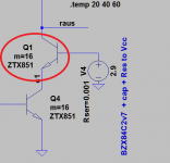
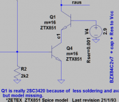
And BTW, using the same expensive ZTX851 for the cascode is a not needed luxury; the cascode device doesn't need to be low noise, it's contribution to the input referred noise is very small. Any medium power device in TO252 and a little bit of PCB copper for cooling will do in that position.
There is no second set of ZTX851, in the text and the photos it is made clear that there is a 2SC3420, for which I have no spice model. I have not seen a case where a cascode added significant noise ever.
The bias regulator is a ZTX851 because the box was on the table.
Why wouldn't you place a separate current setting resistor for each pair? C2 will pick all possible interference
The source resistors are in series to the input and their thermal noise adds directly to that of the transistor. Especially for FETs one would need quite large resistors to have an equalization effect. For bipolars with their higher gm the situation is better, but still bad. You would need huge decoupling caps for each source resistor to get rid of the noise.
For the same reason, gate stoppers are problematic when you are serious abt. noise.
Cheers, Gerhard
But the Lithium pack makes life much easier.
That is somewhat equivocal!

There is no second set of ZTX851, in the text and the photos it is made clear
that there is a 2SC3420, for which I have no spice model. I have not seen a case where
a cascode added significant noise ever.
The bias regulator is a ZTX851 because the box was on the table.
Sorry, I looked at the schematic and wondered...
Attachments
For the same reason, gate stoppers are problematic when you are serious abt. noise.
A friend suggested 1uH in series with each gate. I used 470nH being afraid of turning this into a Colpitts oscillator, works just fine for 8xBF862. Probably damping each 1uH or slightly larger inductor with a 0402 resistor of a few ohms would be even better.
Probably damping each 1uH or slightly larger inductor with a 0402 resistor of a few ohms would be even better.
We would just use a small value RN55 resistor as a form for a few turns of #30 magnet wire.
Another point on the noise IME GR noise has a very strong TC but it matters where you are looking at the spectrum. I wish I had some of my plots of 0.1 to 10Hz noise vs T, since the noise for almost all classic bipolar JFET amps got worse with cooling (including some with a "sweet" spot in T where things went crazy). I also plotted GR noise down to 11uHz to show that it indeed turned into 1/f eventually. I rarely saw as strong a TC with just 1/f noise.
Obviously modern SOI processes don't respond to scratching the back side of the wafer
. You would be surprised at the almost random guesswork process of trying different anneals, gettering with implant damage, etc. goes on. I still have not used up my first tubes of BF862's but I have not seen a 1/f problem (others have reported bad batches).
OK, it's not really PSSR but the indication how much Vcc noise one can afford
without worsening the noise behavior of the amplifier. With 20 pV input referred from Vcc,
and a geometric total of 50, a LT3042 could be justified just so.
But the Lithium pack makes life much easier.
Hmm, back to a napkin calculation, your input stage has 0.8S transconductance (40*200mA) and a voltage gain of 51*0.8~40.
The true PSRR is 1, therefore the power supply noise will appear at the output and will need to have an input referred value of one third of the amplifier's 0.05nV/rtHz to be negligible. Which leads to a power supple with output noise of 0.017*40=2.8nV/rtHz. That is about at the limit for the best ICs today, LT3042/LT3045, and that only @10KHz. At lower frequencies, the power supply noise will affect the overall noise performance, the LT3042 has 60nV/rtHz @ 10Hz or 1.5nV/rtHz input referred. Can't say from your measurements how much has your amp @ 10Hz, but it is likely less that the PS contribution.
So stay with the lithium cells, I don't think you can do better. Also, make sure you are using opamps with less that 1nV/rtHz voltage noise behind the preamplifier, since the output noise is about 2nV/rtHz.
That can be arrived at easier when one leaves out the /gain term in the simulation.
But PSSR is not a value for itself, it is important at which point it hits. 0 dB from 2nV pollution into the bias network would be a complete disaster; 2 op amps later towards the output, we could ignore it. And placing a 30 dB attenuator after the transistor gain stage would improve the PSSR by 30 dB while making the amplifier useless.
I have measured the noise of the batteries already in this thread: < http://www.diyaudio.com/forums/digi...-noise-regulator-dac-clock-3.html#post5350207 > and more types of batteries in < http://www.hoffmann-hochfrequenz.de/downloads/NoiseMeasurementsOnChemicalBatteries.pdf >
The 20 x ADA4898 amplifier has since been upgraded to 220 uF foil plus one 4700 uF wet slug tantalum in the input. The price of the tan really hurts, it dwarfs the price of all op amps or any reasonable number of ZTX851.
BTW the tantals feel really heavy. An alu electrolytic of the same electrical size feels empty when you lift it.
The post amplifier is two ADA4898 stages, one for noise and one for output drive.
This amplifier is more like a test balloon for the chopper amplifier I mentioned above. It used to have 6 ADA4898 op amps after the chopper, but the ADG816 switches have huge charge injection, and that led to offset problems. Somewhere you have to pay for the half ohm resistance.
Now I have made the chopper more symmetrical, with one or two chips for each half of the cycle, in the hope that everything averages out in one 500 KHz clock.
I also have removed the transformers; they created ringing problems without end and energy converted to heat in snubbers is probably missing where it is needed. The cheap voltage gain is gone then, also :-(
So I changed the 4898 to BJTs, which AD may not like I could also use Infineon BFP640 SiGe or so. They also feature 230 pV/rt Hz and their higher 1/f corner would be of no consequence in a chopper.
I shoot for, say, 100pV@ some mHz, even worse would probably be progress.
Cheers & bed time,
Gerhard
But PSSR is not a value for itself, it is important at which point it hits. 0 dB from 2nV pollution into the bias network would be a complete disaster; 2 op amps later towards the output, we could ignore it. And placing a 30 dB attenuator after the transistor gain stage would improve the PSSR by 30 dB while making the amplifier useless.
I have measured the noise of the batteries already in this thread: < http://www.diyaudio.com/forums/digi...-noise-regulator-dac-clock-3.html#post5350207 > and more types of batteries in < http://www.hoffmann-hochfrequenz.de/downloads/NoiseMeasurementsOnChemicalBatteries.pdf >
The 20 x ADA4898 amplifier has since been upgraded to 220 uF foil plus one 4700 uF wet slug tantalum in the input. The price of the tan really hurts, it dwarfs the price of all op amps or any reasonable number of ZTX851.
BTW the tantals feel really heavy. An alu electrolytic of the same electrical size feels empty when you lift it.
The post amplifier is two ADA4898 stages, one for noise and one for output drive.
This amplifier is more like a test balloon for the chopper amplifier I mentioned above. It used to have 6 ADA4898 op amps after the chopper, but the ADG816 switches have huge charge injection, and that led to offset problems. Somewhere you have to pay for the half ohm resistance.
Now I have made the chopper more symmetrical, with one or two chips for each half of the cycle, in the hope that everything averages out in one 500 KHz clock.
I also have removed the transformers; they created ringing problems without end and energy converted to heat in snubbers is probably missing where it is needed. The cheap voltage gain is gone then, also :-(
So I changed the 4898 to BJTs, which AD may not like
I could also use Infineon BFP640 SiGe or so. They also feature 230 pV/rt Hz and their higher 1/f corner would be of no consequence in a chopper.I shoot for, say, 100pV@ some mHz, even worse would probably be progress.
Cheers & bed time,
Gerhard
The 20 x ADA4898 amplifier has since been upgraded to 220 uF foil plus one 4700 uF wet slug tantalum in the input. The price of the tan really hurts, it dwarfs the price of all op amps or any reasonable number of ZTX851.
Gerhard
I see oil exploration mentioned as an app, a good match with the $200 210C in-amps.
I have a board with 8x of them summed but no snubbers .That 210C led me astray, IIRC there is a commercial low noise amplifier from
England with this or a similar type number. I assume you meant an app for the
wet tantalums?
BTW the input caps in the new amplifier are 10*1000u Panasonic organic polymer;
methinks they are quite leaky.
I did not post #424 in this form; that were several smaller posts that have been
compressed into a large one. The pointer to my post in one
of Waly's messages leads now to nirvana. Weird BBS software.
Last edited:
Known "optimization" bug. Seems it can only be avoided by waiting 0.5hrs++ (max edit time) between posts or have another member post in between.I did not post #424 in this form; that were several smaller posts that have been
compressed into a large one. The pointer to my post in one
of Waly's messages leads now to nirvana. Weird BBS software.
I assume you meant an app for the
wet tantalums?
Yes, it was partially a joke since Vishay has that on their data sheet but I don't see the obvious connection between the wet caps and down hole instrumentation (the 210 degrees C spec). There is the similar price tag
.I bought them from AVX, they are a lot cheaper than Vishay, but I just
checked again at DigiKey: If I buy them now, I get them in October.
4700u/25V @ € 69.97 each, plus taxes etc.
But then, transport would cost nothing ( since >60€ ) and they get their stuff
from Thief River Falls to my place usually in less then 40h.
Since wet tantals are known for their low leakage and temperature is the
natural enemy of leakage, high temperature is an expected application.
Last edited:
I bought them from AVX, they are a lot cheaper than Vishay, but I just
checked again at DigiKey: If I buy them now, I get them in October.
4700u/25V @ € 69.97 each, plus taxes etc.
For 100 quid you can get an AVX 50,000uF/6.3V wet tantal from Mouser, not even twice the price of the 4,700uF. They have it in stock. I'm about to order one, just curious how "good" (leakage, leakage tempco, ESL, ESR, Tan d, resonances, frequency response, etc...) these caps really are. They are surprisingly small in size.
TWDE503M006CB0Z0700 AVX | Mouser United Kingdom
They have soared to €144 in the mean time and I could not ignore the 400 mOhm.
BTW who would think that adding a ferrite bead to an amplifier input
(Würth from LTspice lib) would f* up the loop gain of an amplifier so completely.
Damping it with the 5 Ohms makes everything nice again.
I had the hope that I could get rid of the gate voltage divider / coupling C for
the cascode/bootstrap, but the depletion MOSFET is not depleted enough. It leaves
only 1 V at the drain of the input JFETs.
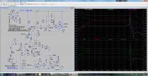
The opened loop goes from V5 to the output of U4. R14 is a first order approximation
of the feedback divider.
and I could not ignore the 400 mOhm.BTW who would think that adding a ferrite bead to an amplifier input
(Würth from LTspice lib) would f* up the loop gain of an amplifier so completely.
Damping it with the 5 Ohms makes everything nice again.
I had the hope that I could get rid of the gate voltage divider / coupling C for
the cascode/bootstrap, but the depletion MOSFET is not depleted enough. It leaves
only 1 V at the drain of the input JFETs.
The opened loop goes from V5 to the output of U4. R14 is a first order approximation
of the feedback divider.
Attachments
- Home
- Design & Build
- Equipment & Tools
- My version of the G = 1000 low noise measurement amp (for Ikoflexer)