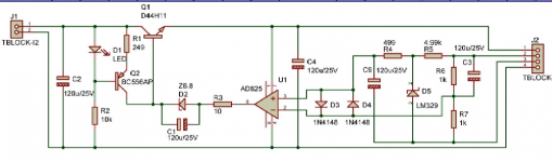
On the zener: if you mean the zener in series with the opamp output, that is there to keep the opamp output somewhere in the middle of the supply voltage so it works correctly. Without it the opamp output would need to be one Vbe below the supply (the base voltage is NOT 6.8V of course - it's one Vbe, some 0.62V - below the emitter which is Vout). Not many opamps would be comfortable with that; it would restrict the opamp choices.
Another benefit of the zener is that it assists in starting up the entire regulation NFB loop when power is first applied. Even if the opamp does crazy things because its supply voltage is too low, the zener guarantees that the series pass transistor's base will be at least Vzener above ground. This allows the regulator Vout to rise up to (Vzener - Vbe), even if the opamp is stupidly and incorrectly slamming its output pin to ground. As long as you choose an opamp whose minimum supply voltage for correct operation, is less than (Vzener - Vbe), the circuit will start up correctly. (In real life of course, the circuit designer chooses an opamp first, then selects a zener such that Vzener >= Vbe + Opamp_min_supply).
Thanks Jan. 'Siphoning' is helpful/descriptive. I asked having read a number of overviews of series pass regulators which simply showed the op-amp output connected directly to the base of the pass transistor.
And the 120uF capacitor across this zener?
Thanks for the help.
EDIT: I 'get' Marks point but it's not the first time I've seen your rationale which I don't follow.
Yes, I mean this zener. Previous to the bootstrapping it was a simple 1N4148 diode fitted with the cathode towards the op-amp output (according to this article). I'm therefore missing why it is necessary to "to keep the opamp output somewhere in the middle of the supply voltage so it works properly". I understand the op-amp with set an output in order to bring its +/- pins to the same voltage with that voltage being set by LM329 (less, presumably the voltage drop across the 499R R4 resistor).On the zener: if you mean the zener in series with the opamp output, that is there to keep the opamp output somewhere in the middle of the supply voltage so it works correctly.
Without it the opamp output would need to be one Vbe below the supply (the base voltage is NOT 6.8V of course - it's one Vbe, some 0.62V - below the emitter which is Vout).
Not many opamps would be comfortable with that; it would restrict the opamp choices.
And the 120uF capacitor across this zener?
Thanks for the help.
EDIT: I 'get' Marks point but it's not the first time I've seen your rationale which I don't follow.
Last edited:
In real life of course, the circuit designer chooses an opamp first, then selects a zener such that Vzener >= Vbe + Opamp_min_supply.
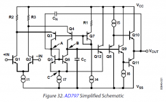
Let's walk through an example using Jan Didden's favorite Lamborghini opamp, the AD797. I've attached its schematic below. We're looking for the minimum supply voltage which allows all transistors in the amplifier to operate -- the opamp doesn't have to rigorously meet all its specs during power-up, it just has to hobble along as a feeble amplifier and to let the NFB loop work. This drives the regulator's Vout upward towards the final output voltage. At sufficiently large Vout (= V_opamp_supply), the opamp does meet all its specs, and the regulator's NFB loop snaps Vout to the correct as-designed output voltage.
We will start by making a few conservative assumptions. By that I mean, assumptions that will give an Opamp_min_supply estimate which is too high rather than too low.
- The voltage drop across R1, R2 and R3, is one VBE
- The voltage drop across current sources I1 thru I7, is one VBE
- All transistors in the signal path have Vce = Vbe, or greater
Path 2: Vcc -> I5 -> Q10 -> Vout -> Q11 -> I6 -> Vss. One VBE across I5, plus one VBE to Q10 emitter (node Vout), plus one VBE to Q11 base, plus one VBE across I6, to Vss. Four VBEs total.
Path 3: Vcc -> R3 -> Q4 -> Q9 -> I6 -> Vss. One VBE across R3, plus one VBE from Q4 emitter to base, Q4 collector (node B) same voltage as Q4 base, plus one VBE across Q9, plus one VBE across I6, to Vss. Four VBEs total.
So we conclude that the AD797 can hobble along and function as some kind of an amplifier, with a supply voltage of 4 x VBE.
The zener diode voltage needs to exceed (VBE + Opamp_min_supply) so we have Vzener > (5 x VBE). Making the conservative assumption that VBE = 0.8 volts, this means we need a zener voltage of 4.0 volts or larger. Walt Jung + Jan Didden's choice of a 6.8V zener, meets the requirement quite nicely.
Attachments
Can one not simply look at the data sheet's minimum power supply operating range, see +/-5V and conclude that a zener >5V is needed?
Anyway, I think we are saying the same thing and I misinterpreted the response. I said "the Zener is there only to ensure the base voltage of the pass transistor is at least 6.8V?" This, of course, was sloppily worded (and likely this response is as well) but what I meant was that it performed no other function than to ensure that there's sufficient bias voltage at the base of the pass transistor such that it can supply sufficient voltage to Vcc. I'm puzzled as to why the diode was needed in the original circuit and what the 120uF cap (C1 on the diyAudio board and C5 in Walt's article) does.
Anyway, I think we are saying the same thing and I misinterpreted the response. I said "the Zener is there only to ensure the base voltage of the pass transistor is at least 6.8V?" This, of course, was sloppily worded (and likely this response is as well) but what I meant was that it performed no other function than to ensure that there's sufficient bias voltage at the base of the pass transistor such that it can supply sufficient voltage to Vcc. I'm puzzled as to why the diode was needed in the original circuit and what the 120uF cap (C1 on the diyAudio board and C5 in Walt's article) does.
... using Jan Didden's favorite Lamborghini opamp, the AD797
Tongue in cheek?
Yes, I mean this zener. Previous to the bootstrapping it was a simple 1N4148 diode fitted with the cathode towards the op-amp output (according to this article). I'm therefore missing why it is necessary to "to keep the opamp output somewhere in the middle of the supply voltage so it works properly".
Ahh but in that case, the opamp supply was not Vout but Vin, which is higher, so the opamp output, even when (almost) directly connected to B of the pass device, was still enough below its supply (Vin) so it works fine.
With moving the opamp supply to Vout, the opamp output pin comes much closer to its supply, too close for comfort, and the zener brings it down some.
Makes sense?
jan
Tongue in cheek?
Actually I remember having quite some discussions with Walt at the time as wether we should recommend the 797 for this particular application, and at the end we did not.
That is not to say that the 797 is not an excellent opamp - it is one on the lowest noise AND lowest distortion opamps I know, and you could build a great MC phono preamp with it.
Jan
Can one not simply look at the data sheet's minimum power supply operating range, see +/-5V and conclude that a zener >5V is needed?
Yes, agreed. My 'about in the mniddle of supply voltage' is a generalization that always works.
Anyway, I think we are saying the same thing and I misinterpreted the response. I said "the Zener is there only to ensure the base voltage of the pass transistor is at least 6.8V?" This, of course, was sloppily worded (and likely this response is as well) but what I meant was that it performed no other function than to ensure that there's sufficient bias voltage at the base of the pass transistor such that it can supply sufficient voltage to Vcc.
I don't think that is true. The current source supplies the current into the B of the pass device to make it operate. I believe this current view is easier to understand than a voltage view.
what the 120uF cap (C1 on the diyAudio board and C5 in Walt's article) does.
Is this the cap across the zener? That is there to make sure that for AC the opamp output is as close to the node it wants to control (B of the pass device) as possible. The zener is only there to offset the opamp output for DC, but for AC you want a direct connection.
Jan
Thanks for the responses Jan. I had just read Walt's article in which he mentioned your 'dissatisfaction' with the AD797 in this application. Hence, I thought the reiteration of the use of the AD797 was a bit 'tongue in cheek'.
I didn't get to spend any more time on this over the weekend. I want to try to get my head around the adjustments needed were one to use a MOSFET in lieu of the BJT pass transistor (I've read the debate earlier in this thread) given the FET gate doesn't draw current (other than leakage) but I need to review a number of things alone first.
I didn't get to spend any more time on this over the weekend. I want to try to get my head around the adjustments needed were one to use a MOSFET in lieu of the BJT pass transistor (I've read the debate earlier in this thread) given the FET gate doesn't draw current (other than leakage) but I need to review a number of things alone first.
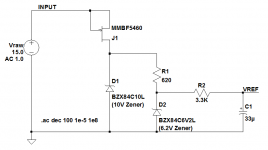
The Super Regulator contains both a negative feedback loop and a positive feedback loop: there's a circuit path from the opamp output back to the opamp Vin- terminal, and there's another circuit path from the opamp output back to the opamp Vin+ terminal. This makes stability analysis and simulation, more difficult.
It occurs to me that adding two more components would let you eliminate the positive feedback loop, making it a lot easier to analyze the Super Regulator for stability. Now the VREF signal is derived from the raw (noisy, ripply) DC input instead of the regulator's output.
The new components are Pchannel Jfet J1, and zener diode D1. They operate as a shunt voltage regulator to generate a 10V power supply. Components R1, R2, D2, and C1 on the attached LTSPICE schematic, exactly correspond to components R5, R4, D5, and C9 respectively, in the Super Regulator schematic.
I've attached a simulation result, showing that input ripple is attenuated by 122 dB at 100 Hz, and it gets better and better at higher frequencies. If you want more attenuation than 122 dB, you can either add another zener and JFET for another stage of regulation upstream of the VREF diode, or else build a cascade of 3-pin regulator ICs to regulate before the VREF diode.
Powering the VREF diode from the raw supply, also solves many of the problems associated with power-on startup in the Super Regulator.
If you decide to play with this idea, please make sure you run the JFET at quite a large drain-to-source voltage: more than 3.5 volts if at all possible. This takes you well past the knee in the IV curve and puts you solidly in the "I am a current source" region of operation. If you select a different JFET, put it up on a curve tracer and find its knee; then bias the thing a comfortable distance away.
Attachments
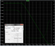
Mark, the increase in suppression with frequency you see is predominantly the result of R2 and C1. Meaning you can get a similar suppression with the same R2/C1 in the original circuit.
Your circuit is good for progressively increasing suppression, but if you would use this circuit in the original circuit, it would be even better, because the supply for this ref is much quieter in the original circuit than with the raw supply you show.
Jan
Your circuit is good for progressively increasing suppression, but if you would use this circuit in the original circuit, it would be even better, because the supply for this ref is much quieter in the original circuit than with the raw supply you show.
Jan
Last edited:
Jan, you didn't grasp that the original circuit contains TWO feedback loops, one of them positive feedback. The proposed modification has a significant major benefit: it completely eliminates positive feedback. It also has a serendipitous, secondary result: at the same time it gets rid of positive feedback, it happens to ALSO attenuate input noise by >120 dB.
I chuckle that the proposed modification is defecated-upon by Walt Jung himself, (HERE). He fails to realize that the loop gain of the positive feedback loop is Av_opamp times the attenuation of the zener's lowpass filter. When you use a mans-man opamp instead of an AD825 (Av = 76dB), the positive feedback loop gain can be greater than 1. This is one under-appreciated reason why the AD797 (Av = 146 dB) doesn't work well in the Super Regulator. The LTC1150 (Av = 180 dB) would be even worse.
I chuckle that the proposed modification is defecated-upon by Walt Jung himself, (HERE). He fails to realize that the loop gain of the positive feedback loop is Av_opamp times the attenuation of the zener's lowpass filter. When you use a mans-man opamp instead of an AD825 (Av = 76dB), the positive feedback loop gain can be greater than 1. This is one under-appreciated reason why the AD797 (Av = 146 dB) doesn't work well in the Super Regulator. The LTC1150 (Av = 180 dB) would be even worse.
Jan, do you have a sim of the noise rejection of the Jung/Didden regulator? Or measured NR? I could and likely should invest the time to model it but perhaps there is something already to hand. It would be nice to have a benchmark for what constitutes "super" NR.
You can see the measured graphs from Jack Walton here: Online Articles scroll down a bit to the 'Jack Walton'graphs.
Jan
Jan, you didn't grasp that the original circuit contains TWO feedback loops, one of them positive feedback. The proposed modification has a significant major benefit: it completely eliminates positive feedback. It also has a serendipitous, secondary result: at the same time it gets rid of positive feedback, it happens to ALSO attenuate input noise by >120 dB.
I chuckle that the proposed modification is defecated-upon by Walt Jung himself, (HERE). He fails to realize that the loop gain of the positive feedback loop is Av_opamp times the attenuation of the zener's lowpass filter. When you use a mans-man opamp instead of an AD825 (Av = 76dB), the positive feedback loop gain can be greater than 1. This is one under-appreciated reason why the AD797 (Av = 146 dB) doesn't work well in the Super Regulator. The LTC1150 (Av = 180 dB) would be even worse.
Ohh I see the pos fb loop alright, that's obvious.
But I don't think your numbers are realistic. Those oscillations I saw with for instance the '797 were always at quite high frequencies, 10's of MHz. At those frequencies, the pos fb loop is pretty much down the drain. And even if it would be an issue it could easily be solved with some more ref filtering like in your new circuit.
If you compare apples with apples (disregarding the pfb for a moment):
Lets assume that you new ref circuit attenuates a ripple on its (the ref circuit) supply 120dB. In your circuit, with the 1V AC 'ripple', that means the ref will have 1uV ripple.
Now connect your new circuit not to the in put raw but to the output, and let us assume that Vo has 1mV ripple. Your ref now has 1nV ripple.
So that's clearly better.
I agree the mechanism is there but I don't think it has the impact you feel it has.
Edit: I looked up the post from Walt you referenced but I don't see him addressing the pfb thing. Can't see anything wrong with that post, unless I miss something?
Jan
Last edited:
If you decide to play with this idea
I'm still trying to figure out how to drive a Mosfet in series pass regulation form (where the reference voltage and Vout are less than Vin).

[I haven't completely abandoned my other reg work (coupled LT1084 and SPX431 or op amp) but I needed a break from trying to get that to settle.]
Yes the JFET and the 10V zener diode form a shunt (pre)regulator which adds another ~ 52 dB of attenuation, no matter what input you drive it with. The JFET's gds is about 0.1 millisiemens and the zener's dynamic resistance is about 25 ohms, giving a voltage divider (attenuator) whose output is 25/10025 of the input. You could attenuate even more, another 15-20 dB, if you used an active zener with a lower dynamic resistance (TL431). But that would be a negative feedback minor loop contained within a positive feedback major loop: bleah! Far more preferable / safer to increase the dynamic resistance of the current source via cascoding. But that would dilute the excellent bang-for-the-buck (2 cheap parts / 52 dB attenuation) you get with the JFET + zener.Now connect your new circuit not to the input raw but to the output
Myself, I prefer to spend this extra 52 dB of attenuation, eliminating the positive feedback loop. I just don't like it. And it gives extra headaches in simulation which I can do without.
I'm still trying to figure out how to drive a Mosfet in series pass regulation form
If you weren't already, just ignore this dribble. It would help if I could finally get through my thick skull which is the drain and which is the source.
If you weren't already, just ignore this dribble. It would help if I could finally get through my thick skull which is the drain and which is the source.
The collector and the emitter
- Home
- The diyAudio Store
- Super Regulator