A gadget made by Spavleski & Zen Mod
Article scribed by Zen Mod
 You’re a Macho Man. You have all the gadgets which real Macho Guys absolutely must have: A CD player, or even a transport with a separate DAC, and recently you made a dedicated media PC, which is dead silent and as capable as HAL 9000! You have nice and potent speakers too. Maybe you also have an ancient Black Disc Spinner, but that's another issue. Or is it? It gives you even more opportunities to later make another gadget, to amplify those tiny signals randomly collected from black grooves...And you just finished making the best amps money can buy, just because you’re lucky, you’re also potent, same as your speakers, and you’re hanging with right Macho Bunch, at the right place, diyAudio, sharing ideas and the newest tips on how to reach Audio Nirvana.
As written above, you’re macho, and you like listening to your music loud, and you also like to watch your fave Football or MotoGP, and actually listening to them, not just staring at a moving picture. There is nothing better than to hear bones cracking (Football) or the metal to asphalt scream (MotoGP)! Wait a minute, you have a Wife, or even a Mom? And they aren’t always in the mood for your torture of loud music every day? So, you really are not so macho and you need a Volume Control. “gotcha!” – JB .
What is important in an Optical Volume Control ?
First, its name must be written with Capital Letters. Second, it must be lossless, unlike those MP3’s, which you hate even more than a Volume Control! Third, it must maintain peaceful coexistence/cooperation with the preceding and following stages at the same time. OK, except for the first, capital letters, the following two aren’t easy tasks to achieve, so now we are going to have to get little more technical...
Everyone here knows what a resistive divider is, so I have no intention of teaching you that just to entertain you. In fact I’m pretty lazy, so I’m typing all this just buying time until I really must paste some schematics and pictures in here, and start to explain a few things. OK, now here’s our first pic, a voltage divider:
Pic. 1
As you can see – that’s pic of a plain ole potentiometer. The Optical Volume Control is however, not made physically of one resistor, with a contact track exposed to a wiper, but from two variable resistors pictured as this:

Pic. 2
These two variable pots are ganged in a way that, while the series one is decreasing in value, the shunt one is increasing in value. To complicate/or simplify things further, imagine that the pots are shaftless (funny term, isn’t it?) and that these two resistors are light-dependent, or better defined, their resistance is inversely proportional to amount of light to which they are exposed. So the pic can look something like this:

Pic. 3
Assuming that we are still following the same law of decrease/increase of series/shunt resistance, it looks that we have gained a couple of things.
1. We have contactless variable resistance, which means that we have succeeded in the first factor needed for losslessness, hehe...
2. We need a proper circuit to make these LEDs behave in the way we want them to exactly. But number two actually has a hidden benefit. We must make some unnecessarily complicated circuit blocks just to preserve the impression that we are still Macho, doing things which our Chicks really aren’t able to understand. The fact that they aren’t even slightly interested in understanding our toyz ‘n’ gamz isn’t part of the prospective of this clever document.
Luckily, thanks to the kind people from the Pro Oriented Industry, who are pretty much unaware of the existence of a bunch of wakoo people obsessed with using real parts for something that is intended to make some funny noises called Music, we have those nice and precious parts: LDRs, or Light Dependent Resistors. For further info on other projects with these funny devices, including GeorgeHiFi’s thread on the Lightspeed Attenuator, see the Links to the side of this article. That boy started the entire Frenzy on Big DiyAudio.
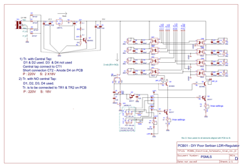
But we boyz from Serbian DiyA, had an idea how to ensure the good behavior of our tiny LDRs with current sources, which must be of course, both adjustable and variable. For the schematic look at “PCB01 Schematic” at the end of this document.
As you can see, we decided to use the old fashioned approach, without the use of fancy add-ons such as microprocessors etc. A pot is still the main adjusting part, but this time we use the cheapest 2x10K linear one, and the audio signal is nowhere near it. Its role is to handle variable voltages, which are steering adjustable Current Sources.
For your convenience, the dedicated power supply schematic is in upper left of schematic sheet. Of course both the PSU and the steering circuit are on the same pcb, accidentally named as PCB01. The supply schematic is pretty self explanatory. Center tapped or non CT transformer, a few diodes, an LM317 as a 70mA CCS, and a few Zener diodes working as a reference for the shunt Darlington on the output. Exact output voltage is the sum of Zener voltages plus 2x the Vbe of Darlington (that’s 1V35). 15V is drawn on the schematic, but who cares if we have 1V35 more...
So, now go back to the exact LDR circuit schematic. If you’re looking at these pages on your ‘puter screen, now is the time to either print these two schematics, or use two screens. Do whatever you wish if you are not ready to jump back and forth, reading text and looking at schematics. Here is what you will discover:
-Q6, along with LED1 and VR1 form a reference voltage string, with 3mA of current flowing through. We have available there two fine voltage points, 2V5 on top of VR1, and ~ 2V more on top of LED1 .
-We are using a reference voltage of 2V5 to inject it into our main Governor (Hasta La Vista - ring a bell ?) Pot itself, so we have nice clean and steady DC voltage to play with. Q3 is any small N type Darlington (or even two small signal diodes connected in series if you’re a cheapskate ) and is nothing other than a convenient voltage shifter. Using it there is to try to null TempCo of the same type Darlingtons used as control elements in two main Current Sources (look down) .
-So, we have clean and steady voltage (2V5 less two Vbe) on top of Pot1. Now look at the vertical string starting from 15V, made of LEDS in 4 LDRs (OK7,5,3,1), closed jumper JMP01, and dedicated Current Source, CS made of Q1 steered with voltage from POT01, cleverly cascoded (by Mighty ZM) with Q4. That one, Q4, is biased from the previously mentioned voltage tap on top of LED1. That vertical string is dedicated to series LDRs.
-I’m clever, so I’ll paste the above paragraph here for the right vertical string, just changing the appropriate part labels. So now look at the vertical string starting from 15V, made of LEDS in 4 LDRs (OK8,6,4,2), closed jumper JMP02, and dedicated Current Source, CS made of Q2 (steered with voltage from POT02), cleverly cascoded (by Mighty ZM) with Q5 . That one, Q5, is biased from the previously mentioned voltage tap on top of LED1. That vertical string is dedicated to shunt LDRs.
Idea is, with the main pot at zero (7 O’clock) position, minimum current is flowing through the left series LDR LED string (on top of Q1) so the mating LD Resistors have max resistance. At the same time, max current is flowing through the right shunt LDR LED string (on top of Q2 ) so the mating LD Resistors have minimum resistance. The result is that our poor tone signal is attenuated maximally.
That crossed behavior is achieved with a crossed connection of reference voltage to a two section of main pot, while the reference voltage is connected to the “start” end of POT02, and it’s connected to “end” end of POT01. Incidentally, at the 12 O’Clock position of the main pot these two voltages coming on both wipers must be same. But we are clever, so we introduce a “fake log law” inducing resistor in each section, R200 and R300. That’s an old trick, to use a linear pot because the section matching of them is better than with cheapskate class logs. Put a few resistors from wiper to ground and Voila!, we have an Audiophool pot for pocket money, or we hope we do at least .... where’s da :devil: smiley when a man needs it ?
OK, now look again at Pic.3.
You see where the signal is coming in, where ground is, and where the signal is coming out. Now, look at the Schematic of PSM LS. We have 4 (or just two, for stereo unbalanced, if you wish so) sections. The first one is made of OK1 & OK2 (R-), the second one is made of OK3 & OK4 (R+), the third one is made of OK5 & OK6 (L-), and the fourth one is made of OK7 & OK8 (L+).
If you obtained your LDRs from me, use Series X and Shunt X as a pair, where X is 1 to 4. So, Series 1 + Shunt 1, Series 2 + Shunt 2, Series 3 + Shunt 3, Series 4 + Shunt 4. They’re matched with that in mind.
I think that everything is clear regarding the points where the signal is coming in, where Ground is, and where the signal is coming out. Just one note: cleverly, on both the schematic and pcb itself, the audio ground isn’t connected to any point of the steering circuit. My Fullrange Bro Spavleski, responsible for those funny patchwork pcbs we made, even uses the top pcb layer as ground for the steering circuit, without any ill effects.
The electrolytic caps and block caps, connected in parallel with LDR LEDs, are there for cleaning up any possible residual noise in the PSU. Use them or not, your choice, they aren’t critical at all.
The P4-P11, 2M2 trimpots are there just in case that the LDRs aren’t tightly matched. If you have tightly matched LDRs you don’t need them at all. Later in this text I’ll explain a better cure, in case you feel or measure that some section is slightly weaker than another.
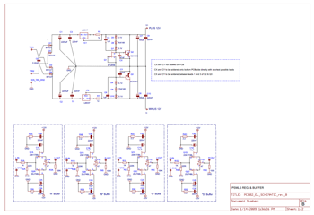
We will leave the Optical Volume circuit now, and look at the buffer schematic; That’s the “PCB02 Schematic”, also on end of this document .
First – look at the the buffer PSU schematic on the top left of the page, when oriented as you’re used to looking at a page and still able to see letters 😉.
Transformer – its wisest to use common one for both Optical Volume and buffer circuits. Whatever. While you’re free to use center tapped or not center tapped transformer for Optical Volume circuit, here you must use a center tapped one, because we need a two-leg supply, where we have both a positive and a negative leg. Of course now, because the power grounds on two circuits/pcbs aren’t connected through any other possible path – you can wire it for PCB01 in any of previously mentioned ways, and for PCB02 you must connect the center tap where it belongs .
The Reg itself, is pretty similar to the already explained reg for Optical Volume. So it’s pretty straightforward; transformer, snubber cap, Graetz diode bridge, electrolytics + solid caps filter for each leg, then LM317 (100mA CCS for pos. leg), LM337 (100mA CCS for neg. leg), then an interesting thing, a sort of common (for both legs) Zener reference string, made of D5,D6,D7,Q1,D8,D9 and D10. The first three are a voltage reference for the shunt darlington Q2, while the last three are voltage reference for the shunt darlington Q3. Q1 is a little CCS for the Zener string, serving both halves, upper and lower, and not being connected to ground.
OK, then we have a string made of Q2 and Q3, and their emitters are connected to output ground, while each Zener string half is finding their potential path/point via the corresponding Darlington. Anyway, to cut the story short, and my pains in explaining things on non-native, you’ll have a pretty low noise reg, with 5V1+0V65+5V1+1V3=13V15 on each output. Twice 5V1 is obviously from the two Zeners, 0V65 is from conducting connected uni diode (1N4148) and 1V3 is 2Vbe of the Darlington.
Stability vs. Time isn’t of much importance here, just because once all parts reach their temperature equilibrium, the output voltage is pretty stable. Conducting connected 1N4148, which have opposite TempCo to Zeners is purely from habit here.
C5 & C6 are noise suppressors for the Zener string. CX and CY are possible oscillation killers and tiniest noise removers. Now I need rofl smilie, but I don’t have it handy 😉. C7,C8,C9,C10 - noise killers, what else ?
Now look lower on the schematic. Pick the one you want of the 4 framed schematic parts, they’re identical. Assuming that you’re looking at the farmost left, that’s nothing other than a JC/Borbely (or Borbely/JC–who knows?) buffer stage, made of two complementary Jfets. Unfortunately they’re the scarce Toshiba ones, but you’re probably so eager to spend a few Greenies making the ultimate Macho Volume Gizmo, that you already have them.
R1A: Usual anti-oscillation/helper/niceplaceformylatestbestbrandofshinyresistor. R2A defines the input impedance of the buffer, and at the same time conveniently taking the gates of both Jfets to ground. Q1A & Q2A, they’re the workers here. Ever see two Woodcutters working with a crosscut saw? They’re doing same thing here, pushing and pulling (Got ya! a crosscut saw can be pulled only 😉 ) their common output, governed by the input signal on their common input. P1A serves as a biasing device for both Jfets, while giving you a chance to adjust the zero offset at the output, after the initial warm-up of these two funny Jfet critters of course.
C4A & R4A , C3A & R5A are snubbers. C1A &C2A are local decoupling, along with snubbers. R3A is there to clamp outputs to ground, even when the outputs have no load. Well, one buffer explained. You must believe me when I say that the other 3 are the same, just differing in parts nomenclature and with the suffix B,C, or D instead of A.
Before taking this writing (for me), and reading(for you) adventure further, lets sum up a few things ...
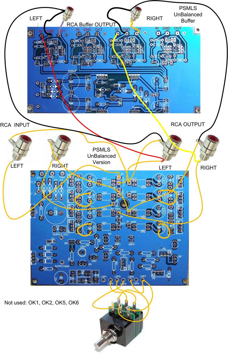
The entire gadget is made of 4 volume blocks on PCB01, called PSM Optical Volume, and 4 buffer blocks on PCB02, called PSM Buffer. We can use/combine them in several ways, and only you can decide the best way to do it. Certainly the simplest way of combining them is a pure balanced attenuator, buffered on the output, meaning that each of 4 volume blocks/channels is buffered on the output.
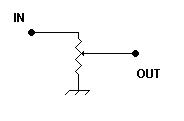
OK, shall we power up the bloody thing(s)? Naah, first we must be sure that you didn’t mess up a few things regarding LDR orientation. Lets look at some nice pics, brought to you courtesy of spavleski. See here:
Be careful! The short (LED) legs are fragile. Even if you have a dot on the LDR body, re-check the dot position with the diode tester on your DVM. The rest of the picture is self–explanatory .
LDR’s are in opposite position in right and left columns. Nota Bene: LDR’s are drawn as photo-transistors on our schematic (now you’re saying before I can: “on end of document, PCB01 Schematic") But don’t worry, the LED’s are drawn the right way.
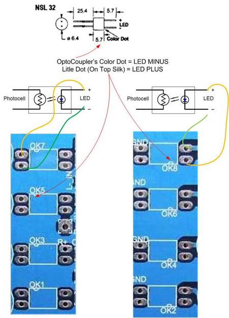
Its now time to ask you – Did you wire that funny pot in this way?
Now is also the time, assuming that you checked twice how the LDR’s are positioned and soldered, and that you already soldered all the other parts (including those funny PC-like jumpers JMP01 and JMP02). There is no need to mount any heatsink now on IC1 and Q7, just check their temperature later with a finger. Warm is OK, if hot then mount some small heatsink of any sort you have in your parts drawer.
Ready for powering up PCB01? Do not connect the transformer leads to PCB02. At this time we need it just for PCB01.
- remove JMP01 and JMP02.
- turn main potentiometer to 12 clock.
- turn mains ON and check PSU voltage. A convenient place for the black probe is any GND point (upper ground plane - LSP1 point ), and for your red probe the upper pin of either JMP01 and JMP02. You’re measuring PSU voltage through the LDR’s LED chain in fact, but that's convenient to check LED’s orientation in same time. Expect voltage of around 16V6. If you’re serious about programmed voltage, change one of the 5V1 Zeners to a 3V9 one, and you’ll be in the 15V ballpark. If that’s the case check few more things:
-Is LED1 shining? if yes, OK (it’s supposed to shine )
-Check the voltage (ref to ground of course) on the middle leg of Q3. It must be around 2V5.
Next, power down and connect a mA meter between the pins of JMP01 with the main potentiometer still in a 12 O’clock position. Then power up. The current is probably few mA. Turn the main pot slowly clockwise, taking care that the current does not rise above 15mA. When you are on max. position with the main pot (5 Clock), set the current to 15mA with P1.
Now power down, remove the mA meter clips from JMP01, place a jumper on it, place the mA clips on the JMP02 pins, and turn the main pot to 12 O’clock. Then power up and check the current. It must be in range of few mA. Turn the main pot slowly anti-clockwise, taking care that the current does not rise above 15mA. When you are on minimum position with the main pot (7 O’clock), set the current to 15mA with P1. Power down, remove the mA meter clips and place the bridge on JMP02. Bingo, you’re done with PCB01 for now.
Shall we progress to PCB02 powering up now?
If you’re finished with that first beer, don’t use another one ..... 😉 If you’re in for another mug of coffee, now is the time.
OK, you can leave the transformer wires connected to PCB01, and you must connect them to PCB02 now. You didn’t forgot to solder one tiny jumper, situated between the two right most 100uF caps and right most 5V1 Zener did you? That jumper is for connecting all ground-planes to actual ground .
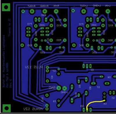
There is one slight omission in PCB02 ; you must solder a wire bridge between two bottom pads – look at the picture – drawn as a yellow line. Its on the rev.B pcb, and we are going to solve that mistake in later pcb issues. Then this note won’t be needed, along with this pic:
You don’t need heatsinks on LM’s and Darlingtons to start. Check later, as I mentioned before. Warm is OK, but if hot mount any small heatsink you have. Pads for buffer Jfets are oriented to ensure a face to pace position of little critters. Feel free to put a small blob of thermal goo between them and tie them with plastic wire tie or even small piece of heatshrink.
Power up da thingie. Check positive and negative PSU rails with the black probe on ground (mid point between two 2200uF caps is convenient place), and red probe to the middle pin of BDX53C for the positive leg, and then red probe to middle leg of BDX54C for the negative leg. If these two voltages are in the ballpark of 12V be happy. Next check DC voltages across every 50R output trimpot. Its fine if you see around 250-300 mV That’s the sign that both Jfets in each buffer are conducting. While you are there, if everything is OK after 10min or so, put black probe on ground, red probe on each ( one at a time) buffer output and adjust DC offset to zero with the trimpot.
Now, you can power off your new Semi-Macho gadget and think of what you really want to make. It’s sorta complicated to describe the several possible variants, so I made few sketches and I hope that things are clearer that way.
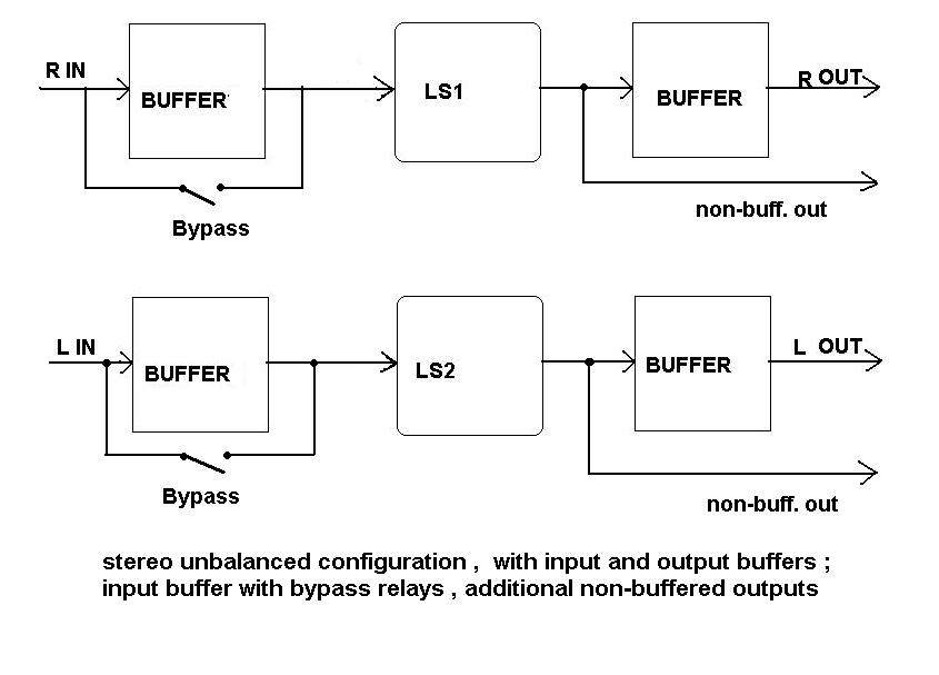
First – full blast ......... nope, just in case, I’ll start with simplest configuration:

It’s pretty obvious that this configuration is for plain stereo attenuation – two attenuator channels, two buffers. That means that each channel output is buffered. It’s handy to have spare pair of outputs so you can add an additional pair of RCA’s and feed them ditto from attenuator outputs, before the buffers.
Next one is somewhat more complicated :
As you can see, two attenuator sections and four buffers. That way each of the stereo unbalanced channels is buffered on both the input and output. Same thinking applicable as in the previous configuration, you can mount an additional pair of RCAs and feed them pre-output buffers . You can also mount a small 2-deck toggle switch on the front panel and bypass the input buffers whenever you feel that’s wise in case that you have one source with enough muscles to drive the LS directly, and other sources that are weaker in driving capability. A toggle switch can be used to control a small relay, which will usually have better contacts than the switch itself, so it’s beneficial to use a relay as a bypass switch. You can steal a few dozens of mA for the relay from the raw PSU before the PCB01 reg. Be creative and find these points, or for a wiser/purist solution, make a small pcb with a tiny Graetz diode bridge and a small electrolytic cap, and put an adequate resistor in line with the relay coil. That way you’ll not pollute any part of the DC grid in the gadget.
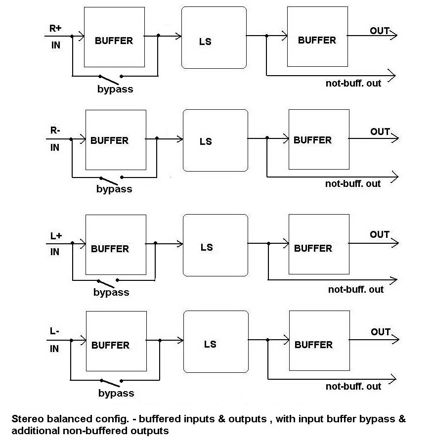
OK, the next one is the (in fact – almost) full blast configuration. A fully balanced attenuator , buffered on output. Look at this:

The picture is pretty self- explanatory, even without the text below 😉
Now, just one final teaser ...... This is what I call full blast!:
You would need two PCB02 boards for that final configuration, and I firmly doubt that anyone needs that, or has the time and will to make it.
Well, while I’m in mood for writing, maybe I can write few words about some final tweaks needed not so much for proper functioning of our PSM LS, but for peace of mind. You’ll need a plain DVM (a ‘scope is even better) and any sort of signal generator. It can be a proper siggene, it can be a tube oldie, it can be a test CD, or a simple PC sine wave proggie output from sound card of crappiest PC you have at home...
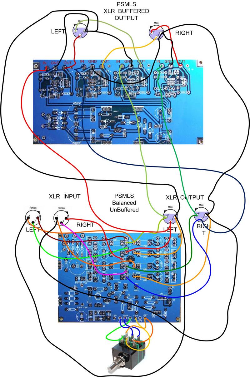
Now I’ll throw in some handy pictures here (courtesy of spavleski) of several most convenient ways of wiring Da Thingie. First the most complicated:
nice place for two pictures. The first one is the crosscut saw in action .... Wood Diy’ers understand this..

if these two are like Jfet buffer then these must be analogous to a cascoded Jfets buffer :
Of course – you can make a mix of XLR/RCA connectors on both ends, input and output, just like in this picture. And I presume that you must know how to wire and mix these two if you’re willing to make gadget like this one:
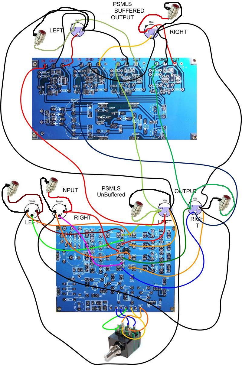
Be warned, this circuit isn’t any sort of balanced/unbalanced or unbalanced/balanced converter. You can use it balanced in/unbalanced out (or vice versa) but you must tie pins 1&3 on the empty XLR while using the adjacent RCA. And yes, I just recently remembered the XLR pin outs, just in case you recently forgot:
Pin 1 – Ground
Pin 2 – Positive Leg
Pin 3 – Negative Leg
Now I can presume that you have decided which arrangement is for you, that you read both the thread and this funny paper, that you wired all needed wires between the transformer, both PCBs, input selector (no, I can’t teach anyone how to wire the selector, hehe), and all input and output connectors, so we are ready for the final procedure.
We need any sort of signal generator, set for ~ 500Hz and a DVM on AC voltage or a ‘scope. I’ll show block schematic for balanced stereo. If you’re using unbalanced stereo, just cover half of the schematic with blank paper. (if you are reading from a screen, tape paper on the screen hehe).
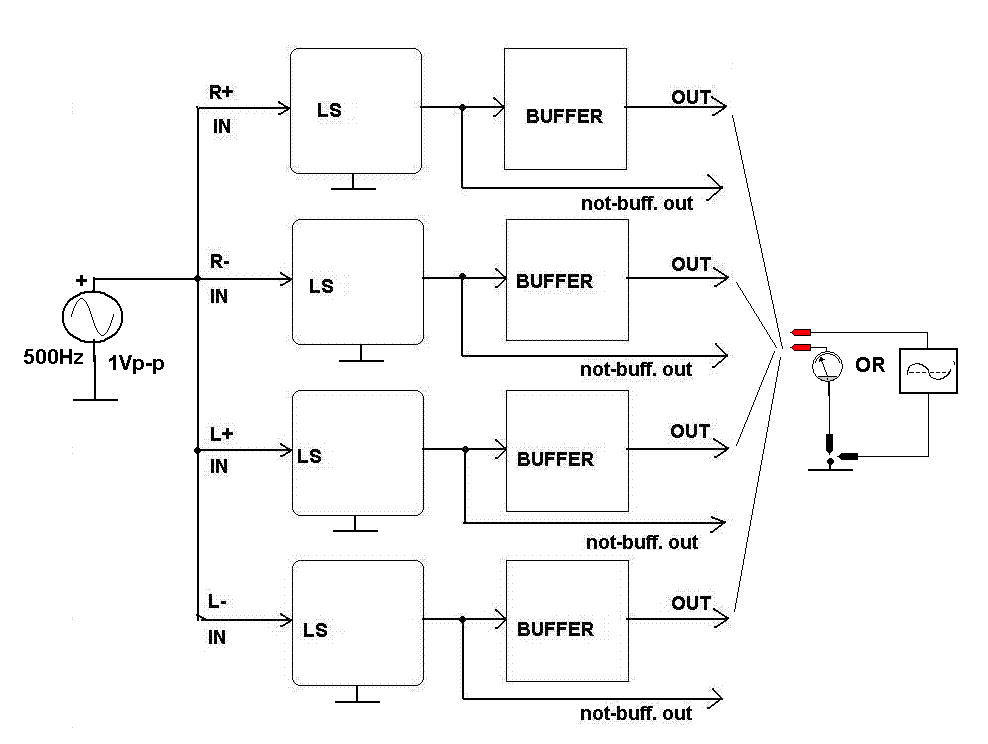
This procedure is brought to all of us by Mighty spavleski 😉. OK – whazzat ?
Nothing other than a signal generator connected to ALL the hot inputs in parallel. Obviously, all input grounds are tied together. That way all 4 channels/sections are fed with the same signal. On right side, connect your AC meter, (either the DVM on AC or a ‘scope) to ground and to one output (HOT) at a time .
Step 1 – position main volume pot on 9 clock; measure Out 1 & write down, measure Out 2 & write down, measure Out 3 & write down, measure Out 4 & write down.
Step 2 - position main volume pot on 12 clock; measure Out 1 & write down, measure Out 2 & write down, measure Out 3 & write down, measure Out 4 & write down.
Step 3 - position main volume pot on 3 clock; measure Out 1 & write down, measure Out 2 & write down, measure Out 3 & write down, measure Out 4 & write down.
Step 4 - position main volume pot on 5 clock; measure Out 1 & write down, measure Out 2 & write down, measure Out 3 & write down, measure Out 4 & write down.
If you’re lucky, all values will be in 5% or even smaller bracket. If not, you have one beautiful trick as a weapon tnx to my clever engineer friend spavleski.
Lets say that 3 channels are pretty equal in attenuation and that one is weaker. Lets say that the weaker channel is channel No.2, intended for R channel, negative leg. If you look on the PCB01 schematic, you’ll see that the LDR responsible for that section is OK1 as series LDR and OK2 as shunt LDR. That channel is weaker than the others IF shunt LDR (OK2) consistently has a smaller resistance than needed. The way to cure that is to steal some current flowing through it. Take a look at this:

I already wrote previously that we are not going to mount these 8 trim pots on PCB01. If you bought them in the meantime, you can curse me, or you can keep them for something else funny, and curse me again.
So now we have a few empty holes in that PCB, and they are a perfectly adequate place for soldering two parallel 3mm red LEDs in parallel with our nasty behaving OK2. That way we are stealing some current from it in the entire range of operation, not just in some narrow area around the desired (listening volume) range, as is case with parallel connected trimpots. This solution is certainly better. Of course you can try for a start, curing it with just one red LED in parallel to OK2, and repeat the procedure as needed. This time you need to just compare the “faulty” channel with the nearest one. If needed, add another LED in parallel to first one.
Now, if you’re using a ‘scope for this procedure, power up once again that signal generator, position the main pot between 7 and 8 clock, connect the ‘scope to any output, and fiddle with P3. The goal is to see just a slight signal wobble on the screen, meaning that we choose a natural position where we can just hear music singing through our new gadget. 7 is zer/nada/zilch/mute, and around 8 is minimum. If you have just a DVM, perform that part of procedure with a signal source connected to input and an amp & speaker on the output when you finally place the PSM LS in your system.
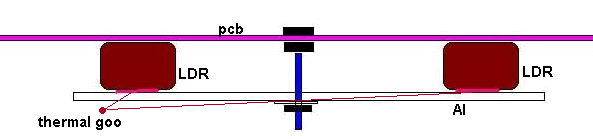
Final notes – to achieve the same thermal conditions for all LDRs, we prepared one nice 3mm hole ditto in center of LDR area. Look at these small pics :

So – I think that the technical part of this text is almost or completely finished. I’ll add a BOM, in fact a list of parts, without a list of places where it is both cheap and clever to buy them. I’m anyway from a different part of world from most of you, and all the parts are probably easy enough for you to get at the nearest Tobacco Store .....
Just few more facts:
Lowest input impedance of LS itself is in range of 350 Ohms, at somewhere around the 9 O’clock position of the pot, while max is up to 35K near both extremes of the pot. The input impedance of the buffer stage is pretty much the same as the input gate(s) resistor, 220K, while output impedance is well in the range of 50 ohms.
PCB01 - PDF Download
PCB02 - PDF Download
------------------------------------------------------------------
Last edited by a moderator:
attentuator.......
diyAudio - diyAudio Articles
 ...... it's so fun - even Mighty ZM couldn't conceive it better
 kudos for at least triple grammar and spell check work ; you boyz are the best

P.S. please - do not edit that announcement
Last edited by a moderator:


This is a great idea. It was also a great idea when Collins used it in their Broadcast Control Boards (AKA Mixers) in 1968 when I was Chief Engineer of WALL in New York. Their original units were plugged into a 7-pin tube socket and were housed in a metal can about 1 inch high. They had incandescent bulbs run by the Pots on the Control Board. Cool: 1 pot could control both channels of the stereo board!
BUT they sometimes failed, and I designed new ones with those really new solid state light thingies. Umm. oh, yeah.. LED's They only cost about $4 apiece. I epoxied them on top of LDR's and put them back in those 7-pin tube plugs. They matched better and were more stable than the original ones..
Hey, they may still be running today.. only 32 years later 🙂
Regards, Terry King ..On the Red Sea at KAUST.edu.sa
terry@terryking.us
Newsletter: Red Sea News Community Information: http://redseainfo.info
🙂
yup - this one is certainly looking as me - sitting on her shoulder

other ones are certainly more cascode-like 😛
yup - this one is certainly looking as me - sitting on her shoulder
other ones are certainly more cascode-like 😛
Last edited:
😉
Dear diyaudio friends,
I just want to underline that the whole idea comes from who the else but "the fugly" 😉 ZM mind. My sincere contribution was a bit on this Project by means of drawing PCB's, schematics and giving comments. Anyhow, having made the prototype of this gadget in balanced mode, my life has been changed, and my searching for the best possible pre-amp finished.
With regards,
spavleski
Last edited by a moderator:

Optical Attenuator Distortion
Neat idea. I have some of these devices so I breadboarded two in series. Enough current through the LEDs (also in series) to make the total resistance 5K more or less. Tap to ground just about 2.5K as expected. Applied 2 volts signal to the pot and measured distortion at the tap. 0.06% distortion at 1 KHz. It is largely third harmonic. This is about ten times the distortion through my home built system from CD all the way through to speaker terminals!
I'll stick with plain old pots, thank you.
kudos for at least triple grammar and spell check work ; you boyz are the best
Toughest editing job so far, but the real ZM still shines through I think
🙂
The BDX53C transistor at power supply section heats up, case worst in split supply whereby it gets heated up tremendously even thru I put up heatsink. CHecked the circuit, all connection properly soldered. Can any one check and share the experience? Thanks
Shunt supply will put all the current through the BDX53, if there is no load connected (that's the worst case for shunt regulator if we're talking about heating). If there is a load, part of the current will flow through it, and part through BDX53.
- Status
- Not open for further replies.
- Home
- General Interest
- diyAudio.com Articles
- The Poor Serbian Man's Optical Attenuator